
Bin Zhang, Pingyang Zeng, Zelin Yang, Di Xia, Jiaxin Zhao, Yaodong Sun, Yufei Huang, Jingcui Song, Jingshun Pan, Huanjie Cheng, Dukyong Choi, Zhaohui Li, "On-chip chalcogenide microresonators with low-threshold parametric oscillation," Photonics Res. 9, 1272 (2021)
- Photonics Research
- Vol. 9, Issue 7, 1272 (2021)
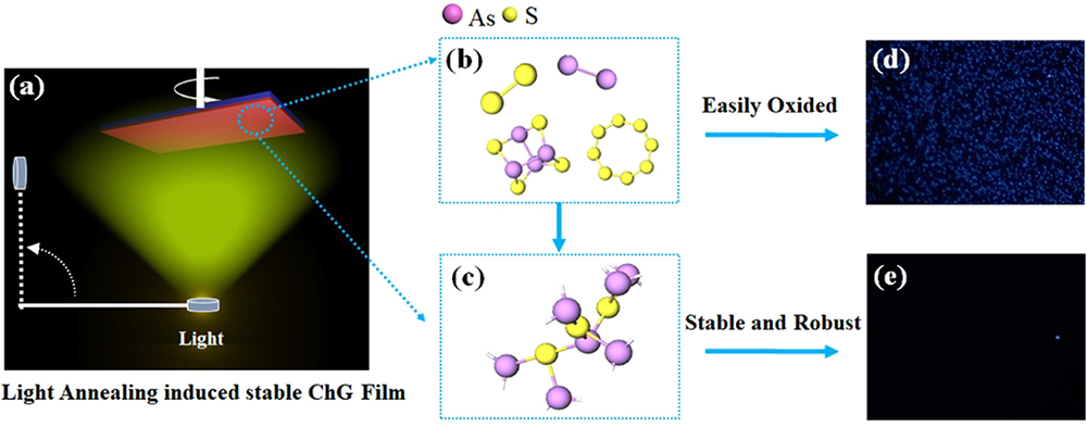
Fig. 1. (a) Schematic of the improved As 2 S 3 in situ light-induced annealing process. The molecular structures of the As 2 S 3 As 2 S 3
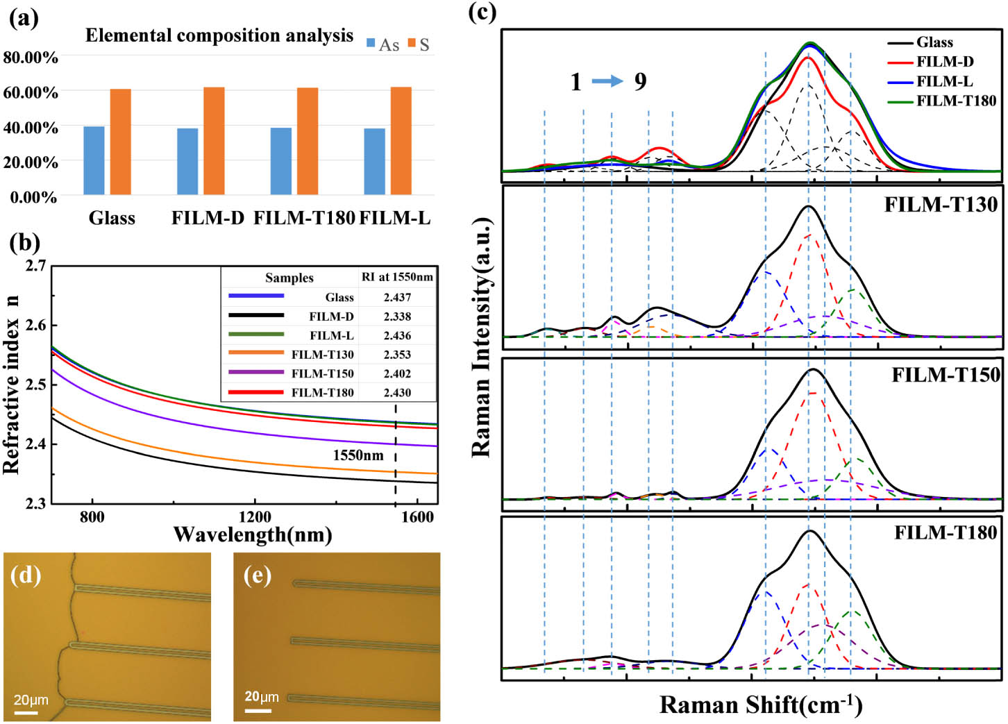
Fig. 2. (a) Composition of As 2 S 3 As 2 S 3 200 mW / cm 2
Fig. 3. Raman Spectra of As 2 S 3 10 mW / cm 2 100 mW / cm 2 200 mW / cm 2 S 8 219 cm − 1 As 2 S 3 As 2 S 3
Fig. 4. 3D AFM scan images of the surface of ChG films: by light annealing under power densities of (a) 10 mW / cm 2 200 mW / cm 2
Fig. 5. (a) Fabrication process for As 2 S 3 / BCB As 2 S 3
Fig. 6. (a) Simulated dispersion of As 2 S 3 TM 00 TM 00 TM 00
Fig. 7. (a) Schematic of the OPO measurement setup. (b) Measured OPO spectrum for input power of 7 mW (TM 00
|
Table 1. Assignments of Raman Shifts Corresponding to the Chemical Bonds in As 2 S 3
|
Table 2. Summary of the RIE and ICP-RIE Conditionsa
|
Table 3. Comparison of the Loss/Q


Set citation alerts for the article
Please enter your email address

© Copyright 2018-2021 | Chinese Laser Press. All Rights Reserved 沪ICP备15018463号-20