• Photonics Research
  • Vol. 9, Issue 7, 1272 (2021)
Bin Zhang1、4、†,*, Pingyang Zeng1、†, Zelin Yang1、†, Di Xia1、†, Jiaxin Zhao1, Yaodong Sun1, Yufei Huang1, Jingcui Song1, Jingshun Pan1, Huanjie Cheng1, Dukyong Choi2, and Zhaohui Li1、3、5、*
Author Affiliations
  • 1Key Laboratory of Optoelectronic Materials and Technologies, School of Electrical and Information Technology, Sun Yat-sen University, Guangzhou 510275, China
  • 2Laser Physics Centre, Research School of Physics, Australian National University, Canberra, ACT 2601, Australia
  • 3Southern Marine Science and Engineering Guangdong Laboratory (Zhuhai), Zhuhai 519000, China
  • 4e-mail: zhangbin5@mail.sysu.edu.cn
  • 5e-mail: lzhh88@mail.sysu.edu.cn
  • show less
    DOI: 10.1364/PRJ.422435 Cite this Article Set citation alerts
    Bin Zhang, Pingyang Zeng, Zelin Yang, Di Xia, Jiaxin Zhao, Yaodong Sun, Yufei Huang, Jingcui Song, Jingshun Pan, Huanjie Cheng, Dukyong Choi, Zhaohui Li. On-chip chalcogenide microresonators with low-threshold parametric oscillation[J]. Photonics Research, 2021, 9(7): 1272 Copy Citation Text show less

    Abstract

    Chalcogenide glass (ChG) is an attractive material for highly efficient nonlinear photonics, which can cover an ultrabroadband wavelength window from the near-visible to the footprint infrared region. However, it remains a challenge to implement highly-efficient and low-threshold optical parametric processes in chip-scale ChG devices due to thermal and light-induced instabilities as well as a high-loss factor in ChG films. Here, we develop a systematic fabrication process for high-performance photonic-chip-integrated ChG devices, by which planar-integrated ChG microresonators with an intrinsic quality (Q) factor above 1 million are demonstrated. In particular, an in situ light-induced annealing method is introduced to overcome the longstanding instability underlying ChG film. In high-Q ChG microresonators, optical parametric oscillations with threshold power as low as 5.4 mW are demonstrated for the first time, to our best knowledge. Our results would contribute to efforts of making efficient and low-threshold optical microcombs not only in the near-infrared as presented but more promisingly in the midinfrared range.

    1. INTRODUCTION

    High-efficient optical nonlinear processes based on high-quality (Q) factor microresonators (MRs) have attracted huge attention for applications such as high-brightness and broadband lasing [1], coherent telecommunication [2], quantum optics [3], and high-precision sensing [4]. High-Q optical microresonators can feature high field confinement, long photon lifetime, and small mode volumes and therefore can dramatically boost the light–matter interaction within the resonators and reduce the power threshold [57]. Among others, chalcogenide glass (ChG) is an attractive material for the study of nonlinear optics because it has broad transparency from the visible to the footprint infrared region (up to ca. 20 μm), high Kerr nonlinearity (10–100 times higher than several typical amorphous materials), low two-photon absorption (TPA), and no free-carrier effects [810]. More importantly, being amorphous, ChG can adhere to different substrates by thermal evaporation at the low glass transition temperature (Tg, less than 300°C) without surface modification or bonding process, which is compatible with a back-end CMOS process [9,11,12]. These advantages make ChGs versatile in numerous applications, including stimulated Brillouin scattering (SBS) [13], SBS oscillation [12,14,15], broadband supercontinuum generation [10], midinfrared parametric amplification [16], Raman amplification [17], and so on. Especially, optical frequency combs based on the optical parametric oscillation (OPO) process can now be implemented on a chip to revolutionize applications in metrology and sensing through optical parametric processes [18,19]. Of particular interest is to implement chip-scale and high-Q microresonators using ChG, which can induce intensive parametric oscillations at low power and can lead to the generation of optical Kerr frequency combs in operational wavelength windows including the midinfrared [12].

    However, ChGs are believed to be unstable and can be easily oxidized. Previously reported ChG MRs usually showed a high level of thermal and light-induced instabilities, which decrease the robustness and efficiency of intracavity OPO [20]. In particular, as-deposited ChG films prepared by thermal evaporation typically contain a lot of homopolar bonds, voids, and subphases compared with bulk glasses. For instance, homopolar As-As bonds in ChG film will easily break and be reconstructed with oxygen when heated or being exposed to lasers in milliwatts [20]. The transformation of such bonds will then lead to the change of the refractive index (RI) and reduce stability of ChG film, which is detrimental to OPO [2022]. As a solution, the thermal annealing process at a temperature close to Tg has been used to promote the conversion of homopolar bonds to heterogeneous bonds and to enhance the stability of ChG film [23]. However, being in the temperature of Tg could also cause cracks in the film during the waveguide fabrication process [21] [also shown in Fig. 2(d)]. As a consequence, a relatively moderate temperature (much lower than Tg) is always chosen to obtain a compromised annealing effect [24]. We had previously proposed a light-annealing process and demonstrated that, when an as-deposited film was subjected to illumination with bandgap light by an array of external halogen lamps, its RI is effectively pushed toward that of the bulk glass, which solved the cracking issue during the thermal annealing [21]. However, the reported film quality remains low compared with that by conventional thermal annealing processes. A possible reason is that, during the transfer process, the film will also be introduced with additional impurity due to the fact that the thermal annealing oven and the thermal evaporation equipment are separated. Up to date, the Q factors of ChG MRs, such as microspheres and microdisks, have been improved up to 107 and 106, respectively [25,26]. However, the highly delocalized optical modes in these ChG MRs render them challenging for compact nonlinear optical parametric applications requiring dispersion engineering [27].

    Generally, the OPO generation in MRs depends on three aspects: 1) the nonlinear figure of merit [FOM, n2/(α2·λ), where n2 is the Kerr nonlinearity, and α2 is the TPA coefficient] of the platform [8]; 2) the high Q-factor and strong modal confinement as well as the large spatial overlap between modes, which are essential for gain to overcome cavity loss [28]; 3) the GVD engineering of the waveguide can achieve simultaneous frequency- and phase-matching among the pump, signal, and idler modes [29]. Over the past years, researches on chalcogenide photonics have focused on the development of new ChG material components with ultrahigh nonlinearity. Yet, it remains challenging to implement high-quality ChG films for the fabrication of integrated nonlinear devices. Thus far, there are few reports on solving chalcogenide films’ stability and realizing the OPO process in ChG MRs [22].

    To address these issues, as shown in Fig. 1, we introduce an in situ light-induced annealing process for post-treatment of ChG films. Here, the typical ChG material, As2S3 with high FOM [12], is selected as the film material to verify the universality of our method [8]. The effects of light-induced annealing and thermal annealing processes are systematically compared on the optical performances of the As2S3 films, including RI, the changes of chemical bonds, surface roughness, and the stability and mechanical stress in the films. Moreover, a systematic fabrication condition was developed to achieve a high Q-factor of more than 1 million in As2S3 microrings with GVD engineering [30]. Owing to the improvements of the materials and fabrication conditions, we experimentally demonstrate, for the first time to our best knowledge, the OPO with a low threshold power of 5.4 mW in the ChG MRs, which paves the path for the nonlinear parametric applications using the ChG MRs.

    (a) Schematic of the improved As2S3 film by an in situ light-induced annealing process. The molecular structures of the As2S3 (b) before and (c) after annealing. The optical microscope images in dark field mode of As2S3 film: (d) oxidated before annealing; (e) maintained stability after the annealing process in the air.

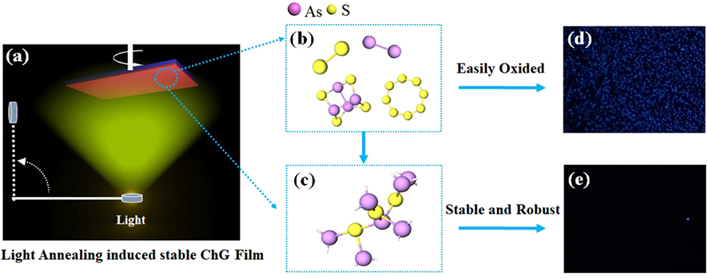
    Figure 1.(a) Schematic of the improved As2S3 film by an in situ light-induced annealing process. The molecular structures of the As2S3 (b) before and (c) after annealing. The optical microscope images in dark field mode of As2S3 film: (d) oxidated before annealing; (e) maintained stability after the annealing process in the air.

    2. EXPERIMENT

    A. Preparation of High Purity ChG Glasses

    High purity elements (99.9999% As and 99.9999% S) were used to prepare the As2S3 glass by the conventional melt-quenching technique. The high purity As2S3 glass was fabricated by a modified physical and chemical purification technique [31]. The purified glass was used as the starting glass for ChG film by thermal deposition.

    B. Preparation and Annealing Post-treatment of ChG Film

    The As2S3 films were deposited on Si substrates with a 3 μm SiO2 layer by thermal evaporation in a vacuum chamber at a base pressure of 7×10⁶Pa [32]. First, the substrate was mounted on a rotation holder and pretreated using Ar plasma to improve the adhesion between the films and substrates. The evaporation rate was set to approximately 5–6 nm/min. Note, the temperature of the substrate was maintained at 30°C during the film deposition process.

    As shown in Fig. 1(a), a power-tunable laser panel with a center wavelength of 532 nm was installed on a screw that could rotate in the deposition chamber. After the film deposition, the laser panel was raised to 5 cm below the film by rotating 90°. Moreover, the ChG wafer loaded on the top of the chamber was rotated with a speed of 20 revolutions/min, and thereby the power densities of the laser panel could be uniform over a full 4 in. diameter wafer. After that, the vacuum was broken, and the wafer was transferred into an atomic layer deposition (ALD) chamber. A passivation layer (Al2O3) with a thickness of 2 nm was deposited on the surface of the chip by ALD, which is to protect the waveguide from moisture. For comparison, a set of 850 nm thick films was put into a vacuum furnace and annealed at different temperatures (e.g.,  130°C, 150°C, and 180°C) for 24 h to ensure molecular bond conversion finishes in the films [21]. After that, the temperature dropped in the furnace with a cooling rate of around 5°C/min. The ChG films were cut into 2cm×2cm for both the light-induced annealing and thermal annealing studies.

    3. RESULTS

    A. Improvement of Stability of ChG Film

    (a) Composition of As2S3 bulk glass, FILM-D, FILM-L, and T180. (b) RI of FILM-D, FILM-L, T130, T150, and T180 as well as the As2S3 bulk glass. (c) Raman spectra of FIML-D, FILM-L, the glass, and films T130, T150, and T180. (Note: FILM-L annealed at the power densities of 200 mW/cm2.) SEM of the waveguide after the electron-beam resist development step with different films: (d) FILM-T; (e) FILM-L.

    Figure 2.(a) Composition of As2S3 bulk glass, FILM-D, FILM-L, and T180. (b) RI of FILM-D, FILM-L, T130, T150, and T180 as well as the As2S3 bulk glass. (c) Raman spectra of FIML-D, FILM-L, the glass, and films T130, T150, and T180. (Note: FILM-L annealed at the power densities of 200  mW/cm2.) SEM of the waveguide after the electron-beam resist development step with different films: (d) FILM-T; (e) FILM-L.

    The Raman and RI spectra of the films by light annealing under different laser intensities of light and duration were measured to achieve optimized parameters of the light-annealing process. As shown in Figs. 3(a)–3(d), the rate of S8 homopolar bond conversions increases as the increasement of power densities of light and the Raman spectra of the three films are gradually approaching a uniform and stable state after 900 min of exposure to the laser. Compared with T180, the light-annealing process can make the film’s RI much closer to bulk glass. Moreover, the FILM-L’s RI is closer to that of bulk glass as the laser power increased. In particular, when the laser intensity is increased to 200mW/cm2, the film’s RI is the same as that of glass, which indicates that higher laser intensity can make the crosslinking of the film molecule close to the bulk glass (Fig. 2). Compared with full thermal annealing process (about 24 h), the light-induced annealing process significantly reduces the annealing time (less than 900 min). As shown in Fig. 4, we measured these films’ roughness, including FILM-L, FILM-D, and FILM-T, through atomic force microscopy (AFM) [27]. The roughness of the T180 (RMS=0.884nm) is significantly higher than that of FILM-D (RMS=0.629nm). However, the roughness of films annealed under different laser intensity conditions (RMS=0.678 and 0.680 nm corresponding to 10 and 200  mW/cm2, respectively) is slightly higher than that of FILM-D. Finally, we chose 200mW/cm2 and 900 min as the light-annealing power density and duration, respectively. To avoid film contamination or degradation during the transfer of the film from the vacuum chamber to the annealing equipment, an in situ light-induced annealing setup is proposed (described in detail the experimental part), where the film is directly annealed by the laser panel in the vacuum chamber.

    Raman Spectra of As2S3 films by light annealing under power densities of (a) 10 mW/cm2, (b) 100 mW/cm2, and (c) 200 mW/cm2. (d) Changes of the S8 bonds at 219 cm−1 in As2S3 films under different power densities of light in 900 min. (e) RIs of As2S3 films by light annealing under different power densities of light after 900 min and FILM-D, FILM-T180 as well as the bulk glass.

    Figure 3.Raman Spectra of As2S3 films by light annealing under power densities of (a) 10mW/cm2, (b) 100mW/cm2, and (c) 200mW/cm2. (d) Changes of the S8 bonds at 219cm1 in As2S3 films under different power densities of light in 900 min. (e) RIs of As2S3 films by light annealing under different power densities of light after 900 min and FILM-D, FILM-T180 as well as the bulk glass.

    3D AFM scan images of the surface of ChG films: by light annealing under power densities of (a) 10 mW/cm2 and (b) 200 mW/cm2; (c) by thermal annealing at the temperature of 180°C. (d) Film as deposited.

    Figure 4.3D AFM scan images of the surface of ChG films: by light annealing under power densities of (a) 10mW/cm2 and (b) 200mW/cm2; (c) by thermal annealing at the temperature of 180°C. (d) Film as deposited.

    B. Reduction of Propagation Loss of ChG Waveguides

    Low-loss on-chip ChG photonic devices are critical for nonlinear photonic applications. Typically, the loss sources of planar waveguides are from the surface interactions and material absorptions [27]. For thermally evaporated ChG films, the material absorptions mainly come from the air’s impurity and oxidized homogeneous bonds. According to the optical microscope images shown in Figs. 1(d) and 1(e), it can be found that there are many bright spots on the surface of FILM-D, which are gradually formed in the air, while FILM-L is highly stable and has not been oxidized. To obtain smooth waveguide sidewalls, we optimize the waveguide fabrication process during etching and post-processing to reduce roughness. Typically, standard waveguide fabrication methods for a ChG waveguide include patterning a masking layer using electron-beam lithography (EBL) or photo-lithography (PL) and transferring this pattern into the waveguide device layer using reactive ion etching (RIE) with fluorine etching gas. Trifluoromethane (CHF3) gas and oxygen (O2) plasma treatment are widely used as etchants in ChG fabrication, and residual resists are removed by inductively coupled plasma reactive ion etching (ICP-RIE) [33]. The roughness of the E-beam resists edge will be transferred to the sidewall, and the fluorocarbon polymer will also be formed and attached to the sidewall during the process. In this paper, a modified waveguide fabrication process, including multipass optimized O2 plasma etching conditions and the waveguide’s thermal reflow process, is shown in Fig. 5(a).

    (a) Fabrication process for As2S3/BCB waveguides. SEM images of (b) cross-sectional and (c) top view of the As2S3 spiral waveguide. (d) Measured propagation losses of ChG waveguides (lines a–c correspond to waveguides with and without the resist as well as with BCB by thermal reflow, respectively). (e) BCB-cladding waveguides at different thermal reflow temperatures (lines a–d correspond to waveguides reflowed at 180°C, 160°C, 120°C, and 140°C, respectively).

    Figure 5.(a) Fabrication process for As2S3/BCB waveguides. SEM images of (b) cross-sectional and (c) top view of the As2S3 spiral waveguide. (d) Measured propagation losses of ChG waveguides (lines a–c correspond to waveguides with and without the resist as well as with BCB by thermal reflow, respectively). (e) BCB-cladding waveguides at different thermal reflow temperatures (lines a–d correspond to waveguides reflowed at 180°C, 160°C, 120°C, and 140°C, respectively).

    Moreover, we investigated the chamber pressure, etching gas flow rate (CHF3), radio-frequency (RF) power, and Ar gas flow rate to determine the optimal etching recipe, as shown in Table 2. Herein, the etching rate of ChG film is 100 nm/min, and the etching selection ratio of ARP6200/ChG configuration is 1:5. The waveguides with a cross-sectional dimension of 2  μm×0.85  μm are fabricated. As shown in Fig. 5(b), after removing the passivation layer on the sidewall surface by the second O2 plasma treatment, the waveguide sidewall is very smooth. For comparison, the insertion losses of ChG waveguides with different lengths of 8, 26.7, 45.4, 64.1, and 82.8 mm were measured using the cut-back method. The microscope image of the ChG spiral waveguide with a length of 82.8 mm is shown in Fig. 5(c). After removing the residual resist, an 82.8 mm spiral waveguide was fabricated with a loss as low as 0.22 dB/cm [as line b in Fig. 5(d)]. Moreover, to verify the effect of thermal reflow, the propagation loss of the BCB-cladding waveguide has been effectively reduced by a thermal reflow process [line c in Fig. 5(d)]. As shown in Fig. 5(e), compared with the loss of waveguides reflowed at 120°C, 160°C, and 180°C, respectively, we can observe the lowest loss of the waveguide by thermal reflowing at 140°C. The loss difference mainly comes from the changes in the roughness of the waveguide surface [27]. The reflow process at low temperature (<140°C) will reduce the roughness of the waveguide surface, while high-temperature treatment (>140°C) will increase surface scattering loss due to internal stress [21]. Therefore, the thermal reflow temperature of the waveguide was set to 140°C. BCB polymer is not the critical factor in reducing propagation loss. We tried other polymer claddings, such as SU-8 2000 and IPG, and achieved similar results. The equal shrinkage coefficient of the ChG core and polymer cladding and moderate thermal treatment can make the waveguide sidewall’s surface smoother. This is a unique method to change the appearance of the ChG device surface [34].

    Summary of the RIE and ICP-RIE Conditionsa

     RIEICP
    ChemistryCHF3:ArAr:CF4:O2
    Pressure (mTorr)1010
    RF power (W)10010
    ICP power (W)300

    RIE is used to fabricate waveguides; ICP-RIE is used to remove resist.

    C. Design and Fabrication of High-Q Dispersion-Engineered ChG Microrings

    (a) Simulated dispersion of As2S3 microring resonator for quasi-TE and TM modes. Insets are calculated TE and TM mode profiles around 1550 nm, respectively. (b) Transmission spectrum of the resonator in the range 1510–1630 nm (TM00). (c) Histogram of intrinsic loss from the measurement of the ChG MR (TM00). (d) One typical resonance with a linewidth of 238 MHz (TM00). SEM images of the top view of (e) microring and (f) enlarged microring section.

    Figure 6.(a) Simulated dispersion of As2S3 microring resonator for quasi-TE and TM modes. Insets are calculated TE and TM mode profiles around 1550 nm, respectively. (b) Transmission spectrum of the resonator in the range 1510–1630 nm (TM00). (c) Histogram of intrinsic loss from the measurement of the ChG MR (TM00). (d) One typical resonance with a linewidth of 238 MHz (TM00). SEM images of the top view of (e) microring and (f) enlarged microring section.

    Table 3 shows the comparison of different ChG platforms for nonlinear photonics. Here, we use the attenuation-related FOMα defined by γ/α [35] and TPA-related figure of merit (FOMTPA, defined by n2/α2λ, β is the TPA coefficient). We should note that fabricating low-loss waveguides and microrings has been demonstrated for several ChGs. At the same time, our works now offer both high FOMα and FOMTPA among dispersion-engineered ChGs devices, and especially the highest value of FOMα has been achieved.

    D. OPO in the High Q-Factor ChG Microrings

    Here, we experimentally demonstrate an OPO process in the improved As2S3 ChG microring. An experimental setup is shown in Fig. 7(a). A continuous-wave (CW) as pump light was generated through a tunable laser (Toptica CTL 1550). The pump light was amplified by an erbium-doped fiber amplifier and subsequently attenuated by a variable optical attenuator to control the input power. The polarization of pump light was aligned with polarization controllers (PCs) to TM polarization of the ChG waveguide. Finally, the output was detected by a photoelectric detector (PD), and the OPO process was shown in an oscilloscope. For OPO measurement, two inverse tapers were fabricated for lensed fiber-chip-lensed fiber couplers to achieve the fiber-to-chip coupling loss of 3.5 dB per facet. The result of the OPO spectrum was recorded by an optical spectrum analyzer. Figure 7(b) shows the OPO spectrum of such a 183 GHz resonator operated at 7 mW, where primary sidebands at ±28-FSR spaced from pump mode can be observed. To determine the threshold power of the OPO process, we measured the output power of the first generated sideband for different pump powers in Fig. 7(c). The threshold power is around 5.41 mW, which is comparable with the calculated threshold power of 5.03 mW by considering this expression [29]: Pth1.54π21ηnn2ω0D1AQl2,where η=Qc/Ql is the coupling factor (Qc, Ql are coupling and loaded quality factor, respectively), n,n2 are linear and nonlinear indices (n2=3.0×10¹⁸  m2/W [8]), D1=2π·FSR, ω0 refers to the angular frequency of pump light, and A is the resonator’s effective mode area. The large Kerr coefficients of the ChG significantly increased the overall Kerr nonlinearity of the device, and the OPO process is significantly enhanced compared with a conventional microcavity of the silica and silicon nitride (Si3N4) with an identical Q-factor [40,41].

    (a) Schematic of the OPO measurement setup. (b) Measured OPO spectrum for input power of 7 mW (TM00). (c) Output power of the first-generated OPO sideband as a function of input power.

    Figure 7.(a) Schematic of the OPO measurement setup. (b) Measured OPO spectrum for input power of 7 mW (TM00). (c) Output power of the first-generated OPO sideband as a function of input power.

    5. CONCLUSION

    An in situ light-induced annealing method was proposed to improve stability and robustness of the ChG films. Moreover, the dispersion-engineered As2S3 microring resonator with a Qin of 1.33 million at 1550 nm was achieved through an improved ChG waveguide fabrication process. In ChG MR with a high Q-factor and stability, an OPO with a threshold power as low as 5.41 mW was experimentally demonstrated for the first time. Our work will promote the on-chip optical parametric amplification and oscillation applications in an ultrabroadband wavelength using ChG MRs with a broad transparency window.

    References

    [1] X. Liu, C. Sun, B. Xiong, L. Wang, J. Wang, Y. Han, Z. Hao, H. Li, Y. Luo, J. Yan, T. Wei, Y. Zhang, J. Wang. Integrated high-Q crystalline AlN microresonators for broadband Kerr and Raman frequency combs. ACS Photon., 5, 1943-1950(2018).

    [2] J. Liu, A. S. Raja, M. Karpov, B. Ghadiani, M. H. P. Pfeiffer, B. Du, N. J. Engelsen, H. Guo, M. Zervas, T. J. Kippenberg. Ultralow-power chip-based soliton microcombs for photonic integration. Optica, 5, 1347-1353(2018).

    [3] M. Kues, C. Reimer, J. M. Lukens, W. J. Munro, A. M. Weiner, D. J. Moss, R. Morandotti. Quantum optical microcombs. Nat. Photonics, 13, 170-179(2019).

    [4] A. V. Muraviev, V. O. Smolski, Z. E. Loparo, K. L. Vodopyanov. Massively parallel sensing of trace molecules and their isotopologues with broadband subharmonic mid-infrared frequency combs. Nat. Photonics, 12, 209-214(2018).

    [5] D. K. Armani, T. J. Kippenberg, S. M. Spillane, K. J. Vahala. Ultra-high-Q toroid microcavity on a chip. Nature, 421, 925-928(2003).

    [6] W. Chen, S. K. Ozdemir, G. Zhao, J. Wiersig, L. Yang. Exceptional points enhance sensing in an optical microcavity. Nature, 548, 192-196(2017).

    [7] X. Shen, R. C. Beltran, V. M. Diep, S. Soltani, A. M. Armani. Low-threshold parametric oscillation in organically modified microcavities. Sci. Adv., 4, eaao4507(2018).

    [8] B. J. Eggleton, B. Luther-Davies, K. Richardson. Chalcogenide photonics. Nat. Photonics, 5, 141-148(2011).

    [9] H. T. Lin, Y. Song, Y. Z. Huang, D. Kita, S. Deckoff-Jones, K. Q. Wang, L. Li, J. Y. Li, H. Y. Zheng, Z. Q. Luo, H. Z. Wang, S. Novak, A. Yadav, C. C. Huang, R. J. Shiue, D. Englund, T. Gu, D. Hewak, K. Richardson, J. Kong, J. J. Hu. Chalcogenide glass-on-graphene photonics. Nat. Photonics, 11, 798-805(2017).

    [10] C. R. Petersen, I. Møller, , B. Zhou, S. Dupont, J. Ramsay, T. Benson, S. Sujecki, N. Abdel-Moneim, Z. Tang, D. Furniss, A. Seddon, O. Bang. Mid-infrared supercontinuum covering the 1.4–13.3 μm molecular fingerprint region using ultra-high NA chalcogenide step-index fibre. Nat. Photonics, 8, 830-834(2014).

    [11] L. Li, H. Lin, S. Qiao, Y. Zou, S. Danto, K. Richardson, J. D. Musgraves, N. Lu, J. Hu. Integrated flexible chalcogenide glass photonic devices. Nat. Photonics, 8, 643-649(2014).

    [12] D.-G. Kim, S. Han, J. Hwang, I. H. Do, D. Jeong, J.-H. Lim, Y.-H. Lee, M. Choi, Y.-H. Lee, D.-Y. Choi, H. Lee. Universal light-guiding geometry for on-chip resonators having extremely high Q-factor. Nat. Commun., 11, 5933(2020).

    [13] B. Morrison, A. Casas-Bedoya, G. Ren, K. Vu, Y. Liu, A. Zarifi, T. G. Nguyen, D.-Y. Choi, D. Marpaung, S. J. Madden, A. Mitchell, B. J. Eggleton. Compact Brillouin devices through hybrid integration on silicon. Optica, 4, 847-854(2017).

    [14] H. G. Winful, I. V. Kabakova, B. J. Eggleton. Model for distributed feedback Brillouin lasers. Opt. Express, 21, 16191-16199(2013).

    [15] T. F. Büttner, I. V. Kabakova, D. D. Hudson, R. Pant, C. G. Poulton, A. C. Judge, B. J. Eggleton. Phase-locking and pulse generation in multi-frequency Brillouin oscillator via four wave mixing. Sci. Rep., 4, 5032(2014).

    [16] S. Xing, D. Grassani, S. Kharitonov, L. Brilland, C. Caillaud, J. Trolès, C.-S. Brès. Mid-infrared continuous-wave parametric amplification in chalcogenide microstructured fibers. Optica, 4, 643-648(2017).

    [17] M. Bernier, V. Fortin, M. El-Amraoui, Y. Messaddeq, R. Vallee. 3.77 µm fiber laser based on cascaded Raman gain in a chalcogenide glass fiber. Opt. Lett., 39, 2052-2055(2014).

    [18] T. J. Kippenberg, R. Holzwarth, S. A. Diddams. Microresonator-based optical frequency combs. Science, 332, 555-559(2011).

    [19] T. J. Kippenberg, A. L. Gaeta, M. Lipson, M. L. Gorodetsky. Dissipative Kerr solitons in optical microresonators. Science, 361, eaan8083(2018).

    [20] D. H. Broaddus, M. A. Foster, I. H. Agha, J. T. Robinson, M. Lipson, A. L. Gaeta. Silicon-waveguide-coupled high-Q chalcogenide microspheres. Opt. Express, 17, 5998-6003(2009).

    [21] D.-Y. Choi, A. Wade, S. Madden, R. Wang, D. Bulla, B. Luther-Davies. Photo-induced and thermal annealing of chalcogenide films for waveguide fabrication. Phys. Procedia, 48, 196-205(2013).

    [22] A. L. Gaeta, M. Lipson, T. J. Kippenberg. Photonic-chip-based frequency combs. Nat. Photonics, 13, 158-169(2019).

    [23] A. El-Sebaii, S. A. Khan, F. Al-Marzouki, A. Faidah, A. Al-Ghamdi. Role of heat treatment on structural and optical properties of thermally evaporated Ga10Se81Pb9 chalcogenide thin films. J. Lumin., 132, 2082-2087(2012).

    [24] B. J. Kim, J. H. Kim, S. H. Hwang, A. S. Budiman, H. Y. Son, K. Y. Byun, N. Tamura, M. Kunz, D. I. Kim, Y. C. Joo. Microstructure evolution and defect formation in Cu through-silicon vias (TSVs) during thermal annealing. J. Electron. Mater., 41, 712-719(2012).

    [25] J. Zhu, M. Zohrabi, K. Bae, T. M. Horning, M. B. Grayson, W. Park, J. T. Gopinath. Nonlinear characterization of silica and chalcogenide microresonators. Optica, 6, 716-722(2019).

    [26] Q. Du, Y. Huang, J. Li, D. Kita, J. Michon, H. Lin, L. Li, S. Novak, K. Richardson, W. Zhang, J. Hu. Low-loss photonic device in Ge–Sb–S chalcogenide glass. Opt. Lett., 41, 3090-3093(2016).

    [27] X. Ji, F. A. S. Barbosa, S. P. Roberts, A. Dutt, J. Cardenas, Y. Okawachi, A. Bryant, A. L. Gaeta, M. Lipson. Ultra-low-loss on-chip resonators with sub-milliwatt parametric oscillation threshold. Optica, 4, 619-624(2017).

    [28] M. Pu, L. Ottaviano, E. Semenova, K. Yvind. Efficient frequency comb generation in AlGaAs-on-insulator. Optica, 3, 823-826(2016).

    [29] T. J. Kippenberg, S. M. Spillane, K. J. Vahala. Kerr-nonlinearity optical parametric oscillation in an ultrahigh-Q toroid microcavity. Phys. Rev. Lett., 93, 083904(2004).

    [30] M. R. Lamont, B. Luther-Davies, D. Y. Choi, S. Madden, B. Eggleton. Supercontinuum generation in dispersion engineered highly nonlinear (γ=10 /W/m) As2S3 chalcogenide planar waveguide. Opt. Express, 16, 14938-14944(2008).

    [31] B. Zhang, W. Guo, Y. Yu, C. Zhai, S. Qi, A. Yang, L. Li, Z. Yang, R. Wang, D. Tang, G. Tao, B. Luther-Davies, P. Lucas. Low loss, high NA chalcogenide glass fibers for broadband mid-infrared supercontinuum generation. J. Am. Ceram. Soc., 98, 1389-1392(2015).

    [32] J. Hu, M. Torregiani, F. Morichetti, N. Carlie, A. Agarwal, K. Richardson, L. C. Kimerling, A. Melloni. Resonant cavity-enhanced photosensitivity in As2S3 chalcogenide glass at 1550 nm telecommunication wavelength. Opt. Lett., 35, 874-876(2010).

    [33] Y. Zhu, L. Wan, Z. Chen, Z. Yang, D. Xia, P. Zeng, J. Song, J. Pan, Y. Feng, M. Zhang. Effects of shallow suspension in low-loss waveguide-integrated chalcogenide microdisk resonators. J. Lightwave Technol., 38, 4817-4823(2020).

    [34] J. J. Kaufman, G. Tao, S. Shabahang, E.-H. Banaei, D. S. Deng, X. Liang, S. G. Johnson, Y. Fink, A. F. Abouraddy. Structured spheres generated by an in-fibre fluid instability. Nature, 487, 463-467(2012).

    [35] M. E. Marhic, P. A. Andrekson, P. Petropoulos, S. Radic, C. Peucheret, M. Jazayerifar. Fiber optical parametric amplifiers in optical communication systems. Laser Photon. Rev., 9, 50-74(2015).

    [36] S. Madden, D.-Y. Choi, D. Bulla, A. V. Rode, B. Luther-Davies, V. G. Ta’eed, M. Pelusi, B. Eggleton. Long, low loss etched As2S3 chalcogenide waveguides for all-optical signal regeneration. Opt. Express, 15, 14414-14421(2007).

    [37] M. J. Collins, A. S. Clark, J. He, D.-Y. Choi, R. J. Williams, A. C. Judge, S. J. Madden, M. J. Withford, M. Steel, B. Luther-Davies, C. L. Xiong, B. J. Eggleton. Low Raman-noise correlated photon-pair generation in a dispersion-engineered chalcogenide As2S3 planar waveguide. Opt. Lett., 37, 3393-3395(2012).

    [38] X. Gai, S. Madden, D. Y. Choi, D. Bulla, B. Luther-Davies. Dispersion engineered Ge11.5As24Se64.5 nanowires with a nonlinear parameter of 136W−1m−1 at 1550nm. Opt. Express, 18, 18866-18874(2010).

    [39] Q. Du, Z. Luo, H. Zhong, Y. Zhang, Y. Huang, T. Du, W. Zhang, T. Gu, J. Hu. Chip-scale broadband spectroscopic chemical sensing using an integrated supercontinuum source in a chalcogenide glass waveguide. Photon. Res., 6, 506-510(2018).

    [40] B. Zhang, Y. Yu, C. Zhai, S. Qi, Y. Wang, A. Yang, X. Gai, R. Wang, Z. Yang, B. Luther-Davies, Y. Xu. High brightness 2.2–12 μm mid-infrared supercontinuum generation in a nontoxic chalcogenide step-index fiber. J. Am. Ceram. Soc., 99, 2565-2568(2016).

    [41] Y. Yu, B. Zhang, X. Gai, C. Zhai, S. Qi, W. Guo, Z. Yang, R. Wang, D. Y. Choi, S. Madden, B. Luther-Davies. 1.8-10 µm mid-infrared supercontinuum generated in a step-index chalcogenide fiber using low peak pump power. Opt. Lett., 40, 1081-1084(2015).

    Bin Zhang, Pingyang Zeng, Zelin Yang, Di Xia, Jiaxin Zhao, Yaodong Sun, Yufei Huang, Jingcui Song, Jingshun Pan, Huanjie Cheng, Dukyong Choi, Zhaohui Li. On-chip chalcogenide microresonators with low-threshold parametric oscillation[J]. Photonics Research, 2021, 9(7): 1272
    Download Citation