• Infrared and Laser Engineering
  • Vol. 50, Issue 8, 20210509 (2021)
Xin Li1, Yong Chen2, Weixian Li1, Yangyang Li3, Lei Zheng2, and Sijin Wu1
Author Affiliations
  • 1School of Instrumentation Science and Opto-electronics Engineering, Beijing Information Science and Technology University, Beijing 100192, China
  • 2Beijing Institute of Space Mechanics & Electricity, Beijing 100094, China
  • 3Daheng New Epoch Technology, Inc, Beijing 100080, China
  • show less
    DOI: 10.3788/IRLA20210509 Cite this Article
    Xin Li, Yong Chen, Weixian Li, Yangyang Li, Lei Zheng, Sijin Wu. Projection aided digital shearography scanning detection technology[J]. Infrared and Laser Engineering, 2021, 50(8): 20210509 Copy Citation Text show less
    Schematic diagram of defect detection
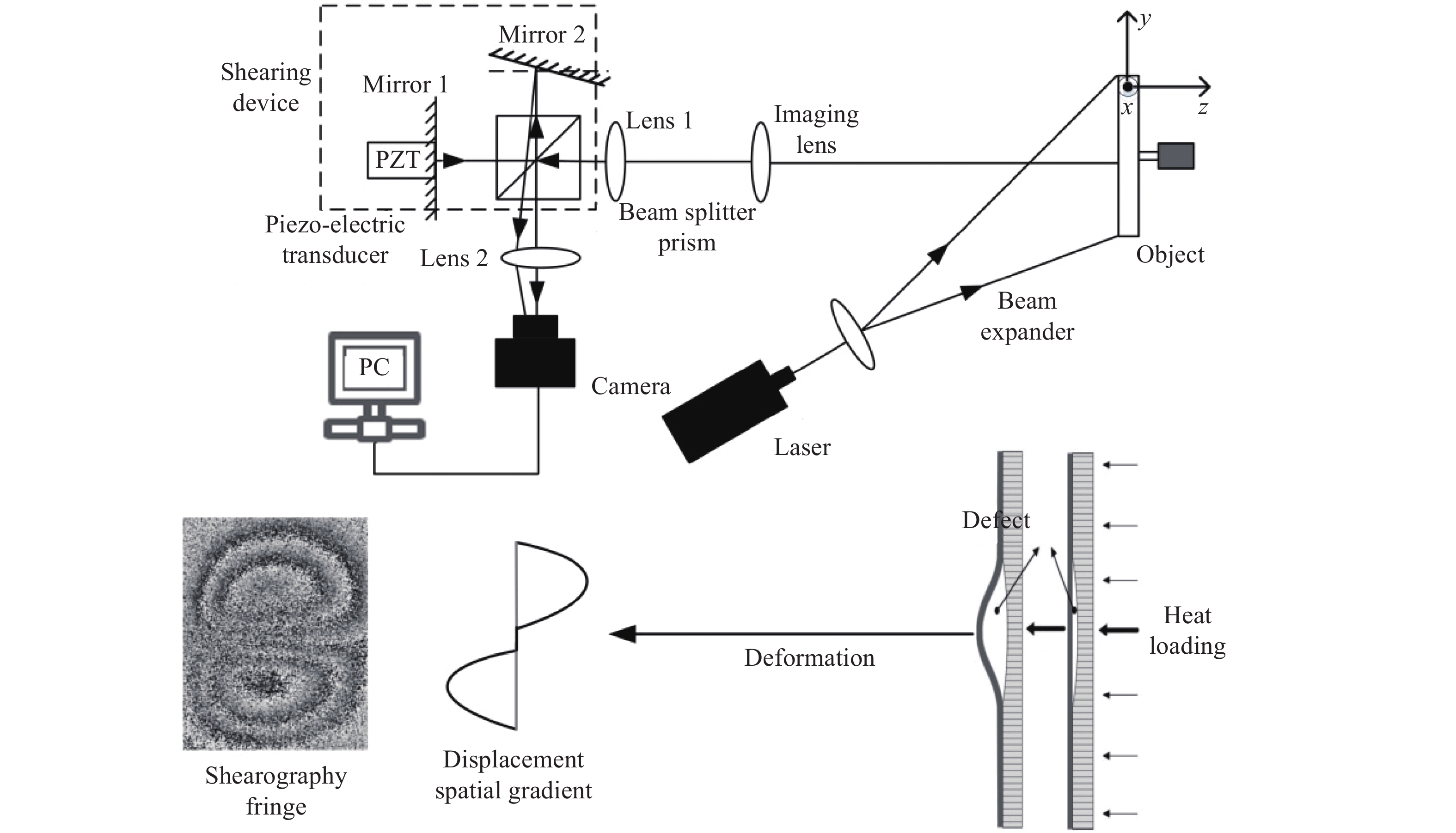
    Fig. 1. Schematic diagram of defect detection
    Image feature. (a) Physical picture; (b) Speckle pattern interferometry; (c) Projection pattern
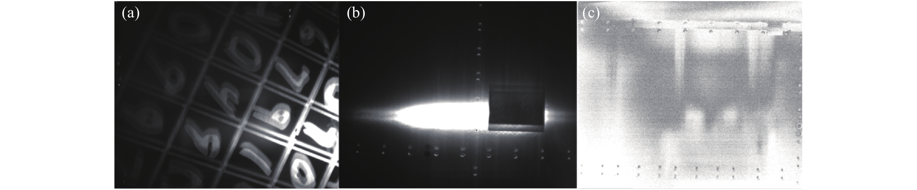
    Fig. 2. Image feature. (a) Physical picture; (b) Speckle pattern interferometry; (c) Projection pattern
    Measuring system
    Fig. 3. Measuring system
    Physical system
    Fig. 4. Physical system
    Projection pattern
    Fig. 5. Projection pattern
    Samples and test results. (a) Sample; (b) Test result
    Fig. 6. Samples and test results. (a) Sample; (b) Test result
    Out-of-plane displacement gradients
    Fig. 7. Out-of-plane displacement gradients
    Projection image. (a) Projection field of view 1; (b) Projection field of view 2; (c) Projection field of view 3; (d) Full-field projection image
    Fig. 8. Projection image. (a) Projection field of view 1; (b) Projection field of view 2; (c) Projection field of view 3; (d) Full-field projection image
    Physical picture. (a) Physical field of view 1; (b) Physical field of view 2; (c) Physical field of view 3; (d) Full-field physical image
    Fig. 9. Physical picture. (a) Physical field of view 1; (b) Physical field of view 2; (c) Physical field of view 3; (d) Full-field physical image
    Speckle pattern interferogram. (a) Interferogram 1; (b) Interferogram 2; (c) Interferogram 3; (d) Full-field interferogram
    Fig. 10. Speckle pattern interferogram. (a) Interferogram 1; (b) Interferogram 2; (c) Interferogram 3; (d) Full-field interferogram
    Split field and full-field images. (a) Sub-field projection image; (b) Sub-field physical image; (c) Sub-field interferogram; (e) Projection image stitching; (f) Physical image stitching; (g) Interferogram stitching
    Fig. 11. Split field and full-field images. (a) Sub-field projection image; (b) Sub-field physical image; (c) Sub-field interferogram; (e) Projection image stitching; (f) Physical image stitching; (g) Interferogram stitching
    NumberDefect location/mmTrue location/mmLocation error/mmDefect size/mmTrue size/mmSize relative error
    1(306.4,93.7)(300.0,100.0)9.033.630.012.0%
    2(403.1,94.6)(400.0,100.0)6.244.740.011.8%
    3(505.1,95.8)(500.0,100.0)6.654.950.09.8%
    4(107.0,198.7)(100.0,200.0)7.152.950.05.8%
    5(206.4,194.9)(200.0,200.0)8.245.440.013.5%
    6(305.7,196.8)(300.0,200.0)6.536.730.022.3%
    7(204.5,297.9)(200.0,300.0)5.028.625.014.4%
    8(305.7,294.8)(300.0,300.0)7.734.930.016.3%
    9(406.9,296.9)(400.0,300.0)7.645.340.013.3%
    10(504.5,298.7)(500.0,300.0)4.756.550.013.0%
    11(105.1,396.2)(100.0,400.0)6.455.750.011.4%
    12(206.4,396.9)(200.0,400.0)7.144.840.012.0%
    13(305.8,397.7)(300.0,400.0)6.233.730.012.3%
    14(407.0,394.9)(400.0,400.0)8.629.025.016.0%
    RMS(5.8,4.0)(0,0)7.04.9013.6%
    Table 1. Defect information
    Xin Li, Yong Chen, Weixian Li, Yangyang Li, Lei Zheng, Sijin Wu. Projection aided digital shearography scanning detection technology[J]. Infrared and Laser Engineering, 2021, 50(8): 20210509
    Download Citation