

Tao Li, Chen Chen, Xingjian Xiao, Ji Chen, Shanshan Hu, Shining Zhu, "Revolutionary meta-imaging: from superlens to metalens," Photon. Insights 2, R01 (2023)
- Photonics Insights
- Vol. 2, Issue 1, R01 (2023)
![Two branches of optical lens evolution towards revolutionary application in the information society, where the representative figures of metamaterials, superlenses, hyperlenses, metalenses, and multilevel diffractive lenses are adapted from Refs. [18,19,21,23,28], respectively.](/richHtml/pi/2023/2/1/R01/img_001.png)
Fig. 1. Two branches of optical lens evolution towards revolutionary application in the information society, where the representative figures of metamaterials, superlenses, hyperlenses, metalenses, and multilevel diffractive lenses are adapted from Refs. [18,19,21,23,28], respectively.
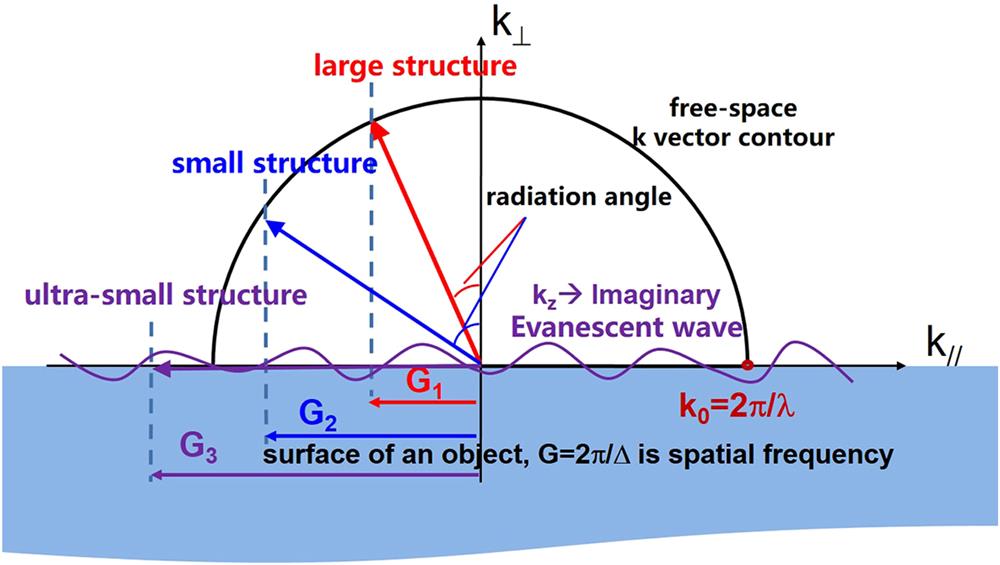
Fig. 2. Schematic (
Fig. 3. (a) Schematic of light focusing (propagating wave) with a slab of NIM; (b) schematic of amplitude evolution of the evanescent wave, showing the recovery inside NIM of the decaying field intensity; (c) electrostatic field of two opaque slits with distances far smaller than the wavelength in the object plane, to be imaged by a silver lens; (d) electrostatic field in the image plane with and without the silver slab in place[17].
Fig. 4. (a) Schematic of the experiment of superlens imaging with 35-nm-thick silver film. (b) An arbitrary object, “NANO,” was imaged by a silver superlens, where the upper panel is the object fabricated in Cr film, middle shows images by Ag superlens, and bottom is the projection results as the Ag superlens is replaced by a PMMA spacer. (c) Detailed line information of the feature size captured by the Ag superlens and without it[19].
Fig. 5. Schematics of light propagations and wave vectors in uniaxial media with principal dielectric constants of different signs[46]. (a) Wave vector diagram (S ) of the transmitted wave indicating the direction of energy flow. (b) Wave vector diagram for a uniaxial medium with
Fig. 6. Several kinds of hyperbolic metamaterials. (a) Negative index material for TM-polarized light realized by silver nanowire array[47]. (b) Hyperlens formed by cylindrical multilayered nanostructures for far-field super-resolution imaging[21]. (c) Multilayered negative index materials working in thin UV wavelength region, where negative refraction properties are measured for TM polarization (right panel)[48].
Fig. 7. Negative refraction in the plasmonic slot waveguide system at visible frequency[50]. (a) SPP dispersions in t 1. (c) SEM image of sample (left panel); experimental results of the positive refraction at
Fig. 8. (a) Waveguide array constituting metallic metasurface for manipulating the surface plasmon wave with (a1) positive dispersion, (a2) zero (flat) dispersion, and (a3) negative dispersion[55]. (b) Simulated symmetric and antisymmetric modes of coupled plasmonic ridge waveguide that gives rise to positive and negative dispersions for the simulation of massless Dirac Fermion[56]. (c) Curved dielectric waveguides in coupling with Bessel type of effective coupling coefficient that gives rise to the simulation of massless Dirac Fermion[60].
Fig. 9. (a) Simulated effective coupling coefficient in densely arranged Si waveguides with a comparison of theoretical Bessel function. (b) Simulated light propagations in all straight waveguides (positive dispersion, top panel), all curved waveguides (negative dispersion, middle panel), and the cascaded one (superlens, bottom panel). (c) Fabricated Si waveguides with ample cascaded segments and fan-out input and output couplers. (d) Experimentally recorded in-plane superlens imaging input from two opposite ports[61].
Fig. 10. Numerical confirmation of all-angle reflectionless negative refraction[63]. (a) Schematic configuration of all-angle negative refraction, where half of the top surface of the Weyl metamaterial is covered by a PEC layer, while the other half is covered by a PMC layer. A point source (electric dipole in
Fig. 11. Design principles of metasurfaces. (a) Schematics of the generalized Snell’s law of refraction[22]. (b) Metasurface with V-shaped antenna array[22]. (c) Gap–plasma metasurface[85]. (d) Huygens metasurface[87]. (e) Propagation phase metasurface[88]. (f) PB phase metasurface[90]. (g) Metasurface with planar chiral meta-atoms[99]. (h) Metasurface with combination of resonant phase and PB phase[26]. (i) Metasurface with combination of propagation phase and PB phase[89].
Fig. 12.
Fig. 13. Multi-wavelength achromatic metalenses. (a) Multispectral achromatic metalens with stacked layers[114]. (b) Spatial segmented achromatic metalens at RGB wavelengths[115]. (c) Dual-wavelength achromatic metalens with polarization manipulation[116]. (d) Achromatic metalens based on waveguide resonance[117]. (e) Bandpass-filter-integrated multiwavelength achromatic metalens[118].
Fig. 14. Broadband achromatic metalenses. (a) Achromatic metalens in reflection mode with a bandwidth from 1200 nm to 1650 nm,
Fig. 15. Fundamental bound of the achromatic metalens[30]. (a) Solutions to extend or break the limits. (b)
Fig. 16. (a) Metalens doublet[25]. (b) Optimized multi-parametric geometries[134]. (c) Monolayer quadratic metalens[141]. (d) Double-layer metalens incorporated with a quadratic metalens and an aperture stop[138]. (e) Extended FOV for microscopy with a metalens array[142]. (f) Wide-angle-imaging camera enabled by a metalens array[143].
Fig. 17. (a) Metalens with
Fig. 18. (a) Ultra-broadband super-oscillatory metalens with sub-diffraction light focusing with focal shift due to dispersion[152]. (b) Achromatic broadband super-resolution imaging with a combination of the metasurface filter and achromatic lens[154]. (c) Supercritical lens with sub-diffraction resolution and corresponding comparison imaging results[156].
Fig. 19. Inverse design and AI algorithms in the metalens design and optimization. (a) Multilayered 2D metalens with aberration corrected under incident angles of 0°, 7.5°, 15°, and 20° based on topology optimization[136]. (b) Dividing the desired phase profile into linear sections with topology optimization for the design of metalens with large area and high efficiency[162]. (c) End-to-end neural imaging pipeline for full-color and wide-FOV imaging[163]. (d) Directly captured images (top row) and aberration corrected images (bottom row) based on AI methods for light-field imaging[164].
Fig. 20. Schematics of metalens roadmap towards high-quality imaging applications.
Fig. 21. (a)–(e) Development of conventional diffractive lenses. The top row shows the schematic of each diffractive lens. The bottom row denotes the height profile of each lens along the black dashed lines. (f) Diffraction efficiency with respect to the diffraction order for a Fresnel zone plate at design wavelength. (g) Diffraction efficiency with respect to the diffraction order for a Fresnel lens at design wavelength. (h) Diffraction efficiency with respect to wavelengths and gray levels for an MDL at first diffraction order. The black dashed line denotes the design wavelength
Fig. 22. Typical examples of achromatic MDLs. (a) 2D broadband AMDL working in the visible region[185]. (b) Broadband AMDL over the visible range from 410 nm to 690 nm with
Fig. 23. Large-scale achromatic flat lens by light coherence optimization[188]. (a) Comprehensive performance P of reported achromatic metalenses and AMDLs with respect to effective thickness
Fig. 24. Typical examples of free-form diffractive lenses applied in other areas. (a) Free-form MDL working at 850 nm with extremely long DOF (5–1200 mm)[189]. (b) Free-form MDL working at RGB (658 nm, 532 nm, 450 nm) with long DOF (2–10 mm)[202]. (c) Free-form diffractive lens over the visible region with large FOV (53°)[182]. (d) Combination of diffractive lenses with deconvolution algorithm[190]. (e) Combination of diffractive lenses with GAN[182].
Fig. 25. Zoom metalens. (a) Tunable metalens on a stretchable substrate and its experimental zoom effect[206]. (b) Focal length tuning with rotational varifocal moiré metalens[207]. (c) Varifocal zoom Alvarez metalens with two cubic metasurface phase plates actuated laterally[209]. (d) MEMS-enabled tunable metalens doublets[210]. (e) Reconfigurable varifocal metalens with optical phase change material[211]. (f) Metalens doublet with functions including camera lens, compound microscope, and Galileo telescope enabled by polarization and distance manipulation[213].
Fig. 26. 3D imaging. (a) Light-field imaging with GaN metalens array and rendered full-color images[198]. (b) Light-field camera with extreme depth of field enabled by spin-multiplexed bifocal metalens array[164]. (c) Ultra-compact snapshot spectral light-field imaging[217]. (d) The metalens depth sensor estimates depth through defocused images by mimicking the jumping spider[219]. (e) Metasurface with engineered point spread function for distance measurements and three-dimensional imaging[220]. (f) Spectral tomographic imaging with aplanatic metalens[132].
Fig. 27. Polarization imaging. (a) Metalens concurrently acting as a quarter-wave plate[221]. (b) Chiral imaging with a metalens[223]. (c) Generalized Hartmann–Shack array of dielectric metalens sub-arrays for polarimetric beam profiling[224]. (d) Polarimetric imaging based on polarization multiplexed metalenses[225]. (e) Portable prototype of the polarization imaging systems enabled by matrix Fourier optics, and the exemplified imaging results[226].
Fig. 28. Meta-microscope implemented by polarization multiplexed metalens array. (a) Two-polarization multiplexed focusing phase design in four lens units. (b) Two groups of sub-images captured by the integrated imaging system with respect LCP and RCP light illuminations. (c) Stitched large FOV (x metalens array covering the whole CMOS. (e) Photograph of metalens imaging chip and (f) implemented meta-microscope with a total size of
Fig. 29. Enhanced microscopy imaging. (a) Nano-optic endoscope for high-resolution optical coherence tomography in vivo [228]. (b) Bijective illumination collection imaging based on metasurfaces and corresponding tissue imaging results[230]. (c) Fourier transform setup for switching between bright-field imaging and phase contrast imaging modes[231]. (d) Spiral metalens for phase contrast imaging[233]. (e) Single-shot quantitative phase gradient microscopy using a system of multifunctional metasurfaces[235].
Fig. 30. (a) Three AMDLs with different diameters and the image of USAF taken from them with the same magnification. The closed blue dashed lines denote the FOV in each figure[188]. (b) Achromatic metalens with diameter equal to 20 µm and the images taken from it[130]. (c) Achromatic metalens with diameter equal to 500 µm and the images taken from it (after image processing)[163]. (d) AMDL with diameter equal to 992 µm and the images taken from it[201]. (e) AMDL with diameter equal to 8 mm and the images (before and after imaging process) taken from it[190]. (f) MDL with diameter equal to 23.4 mm and the images (before and after imaging process) taken from it[182].
Fig. 31. Miniaturization of imaging systems by folding/compressing the working distance. (a) Spaceplate to compress the propagation distance and its imaging results combined with a lens[237]. (b) Operating principle of a pancake metalens. (c) Comparison between pancake optics and pancake meta-optics. (d) Comparison of the experimental setup and imaging results of pancake metalens and normal metalens[239].
Fig. 32. Metalenses with AR/VR applications. (a) See-through near-eye display with a PB phase based metalens[242]; the left is the illustration of the prototype, the middle is the principle of the see-through metalens, and the right is the experimental AR image. (b) Aberration-corrected full-color holographic augmented reality near-eye display using a Pancharatnam–Berry phase lens[243]. (c) Full-color VR/AR display with RGB-achromatic metalens[244]. (d) Illustration of an AR headset with multifunctional nonlocal metasurfaces as optical see-through lenses[252].
|
Table 1. State-of-the-Art Performances and Related Parameters of Reported Achromatic Flat Lens.
|
Table 2. Characteristics of Superlens, Hyperlens, Metalens, and MDL for Imaging.
Mind map for the review


Set citation alerts for the article
Please enter your email address

© Copyright 2018-2021 | Chinese Laser Press. All Rights Reserved 沪ICP备15018463号-20