Abstract
Over the past decades, photonics has transformed many areas in both fundamental research and practical applications. In particular, we can manipulate light in a desired and prescribed manner by rationally designed subwavelength structures. However, constructing complex photonic structures and devices is still a time-consuming process, even for experienced researchers. As a subset of artificial intelligence, artificial neural networks serve as one potential solution to bypass the complicated design process, enabling us to directly predict the optical responses of photonic structures or perform the inverse design with high efficiency and accuracy. In this review, we will introduce several commonly used neural networks and highlight their applications in the design process of various optical structures and devices, particularly those in recent experimental works. We will also comment on the future directions to inspire researchers from different disciplines to collectively advance this emerging research field.
1. INTRODUCTION
Novel optical devices consisting of elaborately designed structures have become an extremely dynamic and fruitful research area because of their capability of manipulating light flow down to the nanoscale. Thanks to the advanced numerical simulation, fabrication, and characterization techniques, people are able to design, fabricate, and demonstrate dielectric and metallic micro- and nano-structures with sophisticated geometries and arrangements. For instance, metamaterials and metasurface comprising subwavelength structures, called meta-atoms, can show extraordinary properties beyond those of natural materials [1]. Many metadevices have been reported that offer enormous opportunities for technology breakthroughs in a wide range of applications including light steering [2–5], holography [6–9], imaging [10–14], sensing [15–17], and polarization control [18–21].
At present, we can handle most of the photonic design problems by accurately solving Maxwell’s equations using numerical algorithms such as the finite element method (FEM) and finite-difference time-domain (FDTD) method. However, those methods often require plenty of time and computational resources, especially when it comes to the inverse design problem aiming to retrieve the optimal structure from target optical responses and functionalities. In the conventional procedure, we normally start with full-wave simulations of an initial design based on the empirical knowledge and then adjust the geometric/material parameters iteratively to approach the customer-specific requirements. Such a trial-and-error process is time consuming, even for most experienced researchers. The initial design strongly relies on our experience and cognition, and usually some basic structures are chosen, including split-ring resonators [22,23], helix [24], cross [25], bowtie [26], L-shape [2], and H-shape [27,28] structures. Although it is known that a specific type of structures can produce a certain optical response (e.g., strong magnetic resonance from split-ring resonators and chiroptical response from helical structures), sometimes the well-established knowledge may limit our aspiration to seek an entirely new design that is suitable for the same applications or even more complicated ones when the traditional approach is not applicable.
Artificial neural networks (ANNs) provide a new and powerful approach for photonic designs [29–37]. ANNs can build an implicit relationship between the input (i.e., geometric/materials parameters) and the output (i.e., optical responses), mimicking the nonlinear nerve conduction process in the human body. With the help of well-trained ANNs, we can bypass the complicated and time-consuming design process that heavily relies on numerical simulations and optimization. The functions of most ANN models for photonic designs are twofold: the forward prediction and inverse design. The forward prediction network is used to determine the optical responses from the geometric/material parameters, and it can serve as a substitute for full-wave simulations. The inverse design network aims to efficiently retrieve the optimal structure from given optical responses, which is usually more important and challenging in the design process. One main advantage of the ANN models is the speed. For example, producing the spectrum of a meta-atom from a well-trained forward prediction model only takes a few milliseconds, orders of magnitude faster than typical full-wave simulations based on FEM or FDTD [38–40]. In the meantime, the accuracy of the ANN models is comparable with rigorous simulations. For instance, the mean squared loss of spectrum prediction is typically on the order of to [40,41]. Moreover, ANNs can unlock the nonintuitive and nonunique relationship between the physical structure and the optical response, and hence potentially enlighten the researchers with an entirely new class of structures.
Sign up for Photonics Research TOC. Get the latest issue of Photonics Research delivered right to you!Sign up now
Solving the photonic design problem by ANNs is a data-driven approach, which means a large amount of training sets with both geometric/material parameters and optical responses are needed. Once the ANN model works well on the training data set, it can be tested on a test set or real problem. The test and training data sets should be in the same design framework but contain completely different data. The general workflow for a forward prediction network includes four steps. First, a large number of input structures and output optical responses are generated from either simulations or experiments. In most of the published works, the amount of data is on the order of . It is noted that the performance of the neural networks depends on both the size and quality of data. To improve the quality of training data, some researchers have applied rule-based optimization methods in the generation of initial training data [42] or attempted to progressively increase the dimension of the training data with the new ones from the trained model [43]. Then we design the ANNs with a certain network structure, such as fully connected layers (FCLs)-based neural networks or convolutional neural networks (CNNs). Next, the training data set is fed into the network, and we optimize the weight and bias for each node. Finally, the well-trained ANNs can be used to predict the response of other input structures that are outside the training and test data sets. As for the inverse design problem, one can simply reverse the input and output and use a similar network structure. However, for some problems, it requires complex methods and algorithms.
This review is devoted to the topic of designing photonic structures and devices with ANNs. We will focus on very recent works on this topic, especially the experimental demonstrations, after introducing the widely used ANNs. The remaining part of the review is organized as follows. In Section 2, we will discuss the basic FCLs and their application in the prediction of design parameters. Then, in Section 3, we will focus on the CNNs that are used in the retrieval of much more complicated structures described by pixelated images. In Section 4, other useful and efficient hybrid algorithms by combining deep learning and conventional optimization methods for photonic design will be discussed. In the last section, we will conclude the review by discussing the achievements, current challenges, and outlooks in the future.
2. PHOTONIC DESIGN BY FULLY CONNECTED NEURAL NETWORK
A. Introduction of FCLs
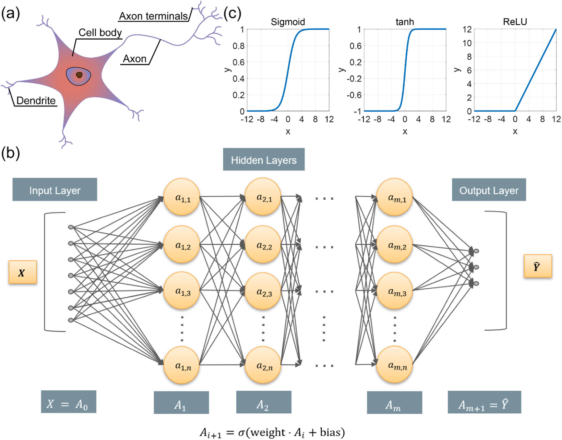
Figure 1.(a) Illustration of a biological neuron. (b) FCLs-based neural network, in which all neurons in adjacent layers are connected. (c) Three widely used activation functions: Sigmoid, tanh, and ReLU.
The training process of the fully connected neural network is quite straightforward. The training set contains an input vector and an output vector ( can be a vector of complex/real values for regression problems or vector of discrete integers as labels for classification problems). The performance of the model is highly dependent on the quantity and quality of the training data set. During the training process, the network first takes the vector as input and calculates the output through the tensor operation and activation from left to right. Then a loss function (or cost function) is defined and needs to be minimized in order to calculate the performance of the neural network. For instance, we can use mean-squared-error (MSE) for regression problems and cross-entropy loss for classification problems. The next step, the backpropagation of error, is the most critical part of ANNs. In the ANN, there are a series of learnable parameters to be optimized, i.e., the weight and bias of each layer. We can then derive the partial derivative of the loss with respect to each parameter . To calculate those values, we need to apply the chain rule layer by layer from the end of the ANN to the front. This is why the process is called “backpropagation.” Finally, all the parameters are optimized by the stochastic gradient descent method: Here the learning rate is a hyperparameter that is usually controlled by the user and is not learnable. The training process is iterated until the loss is minimized. Different learning rates would result in different situations: a large learning rate will cause issues for the model to converge, while a small learning rate will increase the training time of the model. Therefore, the general approach is to assign a large learning rate at the beginning of the training, and after the model is trained for several epochs, the learning rate can be tuned to a smaller value.
B. Design Parameterized Structure by FCLs-Based ANNs
![(a) Top: Schematic of the tandem neural network and SiO2 and Si3O4 multilayers. Bottom: Two examples of target spectra (blue solid lines) and simulated spectra of retrieved structures (green dashed lines). The target spectra are in a Gaussian shape. (b) Left: Predicted (open circles) extinction cross section of the electric dipole (red) and magnetic dipole (black) of core-shell nanoparticles. The solid lines are target responses. Right: Simulated extinction spectra and the corresponding electric field distribution of core-shell nanoparticles. (c) Top: Simulation result and inverse design prediction of the scattering cross section of core-shell nanoparticles. Bottom: Runtime comparison between the conventional method and neural network. (d) Top: A multilayer structure composed of Si3N4 and graphene. Bottom: Optical response of the designed nanostructures (with either low/near-unity absorbance in graphene) under the excitation of s-polarized light. (a) is reproduced from Ref. [46] with permission; (b) is reproduced from Ref. [47] with permission; (c) is reproduced from Ref. [38] with permission; (d) is reproduced from Ref. [48] with permission.](/Images/icon/loading.gif)
Figure 2.(a) Top: Schematic of the tandem neural network and and multilayers. Bottom: Two examples of target spectra (blue solid lines) and simulated spectra of retrieved structures (green dashed lines). The target spectra are in a Gaussian shape. (b) Left: Predicted (open circles) extinction cross section of the electric dipole (red) and magnetic dipole (black) of core-shell nanoparticles. The solid lines are target responses. Right: Simulated extinction spectra and the corresponding electric field distribution of core-shell nanoparticles. (c) Top: Simulation result and inverse design prediction of the scattering cross section of core-shell nanoparticles. Bottom: Runtime comparison between the conventional method and neural network. (d) Top: A multilayer structure composed of and graphene. Bottom: Optical response of the designed nanostructures (with either low/near-unity absorbance in graphene) under the excitation of s-polarized light. (a) is reproduced from Ref. [46] with permission; (b) is reproduced from Ref. [47] with permission; (c) is reproduced from Ref. [38] with permission; (d) is reproduced from Ref. [48] with permission.
Subsequent works have further confirmed the good performance of the tandem network architecture. For instance, S. So et al. used a similar ANN structure to design core-shell structures (with three layers) that support strong electric and magnetic dipole resonances [47]. The ANN was built to learn the correlation between the extinction spectra and core-shell nanoparticle designs, including the material information and shell thicknesses. In Fig. 2(b), the predicted (open circles) extinction cross sections of the electric dipole (red) and magnetic dipole (black) of core-shell nanoparticles are compared with the target responses (solid lines). It is clear that both the electric dipole and magnetic dipole spectra of the designed core-shell nanoparticles fit well with the expectations. J. Peurifoy et al. also studied the inverse design with ANNs for multilayered particles (up to eight layers), with a focus on the scattering spectra [38]. The FCLs were used in both forward prediction of scattering cross-section spectra and the inverse design from the spectra. Using a model trained with 50,000 training data, they can achieve a mean relative error of around 1%. One example is shown in the top panel of Fig. 2(c), in which the result from the neural network is compared with numerical nonlinear optimization as well as the desired spectra. The comparison demonstrates that the neural network model performs better in this design problem. Moreover, the running time of the ANNs-aided inverse design is shortened by more than 100 times in comparison with full-wave simulation as demonstrated in the bottom panel of Fig. 2(c). This result clearly shows the advantage of ANNs in terms of efficiency.
Besides the tandem network, other approaches have been introduced to improve the performance of the FCLs-based neural network. In 2019, Y. Chen et al. employed an adaptive batch-normalized (BN) neural network, targeting the smart and quick design of graphene-based metamaterials as illustrated in the top panel of Fig. 2(d) [48]. Specifically, a layer using an adaptive BN algorithm is placed before each hidden layer to overcome the limitation of BN in small sampling spaces. In the adaptive BN network, it takes activation of each neuron in a minibatch B, batch normalization parameters , , and adaptive parameters , as the inputs. The outputs of the system are the new activation for each neuron. The authors tested their method by deriving the thickness of each layer in the structures. Prediction accuracy of over 95% was achieved. The bottom panel of Fig. 2(d) plots the optical responses of two different examples with varied absorbance in graphene, showing excellent accordance between the target and design responses.
Figure 3.(a) Left: Schematic illustration of the metasurface, the unit cell, and matrix encoding method. Right: Predicted S-parameter and absorptivity with the REACTIVE method. (b) Illustration of the neural network architecture consisting of BaseNet and TransferNet. (c) The trend of spectrum error when layers are transferred to the TransferNet and the predicted transmission spectra for two examples. (a) is reproduced from Ref. [39] with permission; (b) and (c) are reproduced from Ref. [49] with permission.
Due to the data-driven nature of deep learning, the performance of a well-trained ANN highly relies on the training set, and the prediction loss is likely to increase as the inputs deviate from the training set. Therefore, a challenge in the deep-learning-aided inverse design lies in extending the capability of ANNs to an alternated data set that is very different from the training data. Usually, one needs to generate an entirely new training set for similar but different physical scenarios. In this context, reducing the demand for computational data is an efficient way to accelerate the training of deep learning models. Y. Qu et al. proposed a transfer learning method, which is schematically illustrated in Fig. 3(b), to migrate knowledge under different physical scenarios [49]. The prediction accuracy is significantly improved, even with a much smaller data set for new tasks. Two sets of ANNs are involved in this work. The first one, named BaseNet, is trained with initial data. The second one, called TransferNet, copies the first layers from the BaseNet, and the entire system is fine-tuned simultaneously. The authors first transferred the spectra prediction task from a 10-layer film to an 8-layer film, where the source and target task were trained with 50,000 and 5000 examples, respectively. Comparing to direct learning, the result is good enough since the error drops when increases as shown in Fig. 3(c). The TransferNet is applicable for different structures, ranging from multilayer nanoparticles to multilayer films. Based on the model, a multitask learning scheme was studied, which combined the learning for multiple tasks at the same time. It was shown that the neural network in conjunction with the transfer learning method can produce more accurate predictions.
The FCLs have also been utilized in reinforcement learning [50–53], which is another hot area of machine learning, for the inverse design problem. Reinforcement learning has already achieved great performance in robotics, system control, and game-playing (AlphaGo). Instead of predicting the optimized geometry, the ANNs in reinforcement learning behave as an iterative optimization method. In each step, an action to optimize the geometry parameters is predicted. For instance, the action can be increasing or decreasing several parameters by a certain value. The advantage of this approach is that it can be adaptive to specific problems, and it can provide guidance for conventional trial-and-error optimization methods.
Figure 4.(a) Left: Architecture of the proposed neural network for nonlinear layers. Right: Predicted, simulated, and measured transmission spectra of two gold nanostructures under different polarization conditions. (b) Left: Illustrations of MANN used for reconstruction of 3D vectorial field. Right: Experimental approach and characterizations of 3D vectorial holography based on a vectorial hologram. (c) Left: Schematic of a deep-learning-enabled self-adaptive metasurface cloak. Right: Demonstration of the self-adaptive cloak response subject to random backgrounds and incidence with varied angles and frequencies. (a) is reproduced from Ref. [54] with permission; (b) is reproduced from Ref. [63] with permission; (c) is reproduced from Ref. [64] with permission.
In addition to spectrum prediction [55,56], the FCLs-based ANNs have also been used in the inverse design to realize other functionalities and benefit real-world applications [57–62]. Holographic images, for example, can be optimized by ANNs to achieve a wide viewing angle and three-dimensional vectorial field as recently demonstrated by H. Ren et al. [63]. They used a network named multilayer perceptron ANN (MANN), which was composed of an input layer fed with an arbitrary three-dimensional (3D) vectorial field, four hidden layers, and an output layer for the synthesis of a two-dimensional (2D) vector field. There are 1000 neurons within each hidden layer. The scheme of this ANN is shown in the top left panel of Fig. 4(b). The authors showed that an arbitrary 3D vectorial field can be achieved with a 2D vector field predicted by the well-trained model. A 2D Dirac comb function was then applied to sample the desired image. Subsequently, digital holography, calculated from the desired image, was combined with the 2D vector field. This process can be visualized in the right panel of Fig. 4(b). With a split-screen spatial light modulator that independently controls the amplitude and phase orthogonal circularly polarized light, any desired 2D vector beam can be generated. As a result, the experimentally measured image from the hologram can show four different 3D vectorial fields in different regions as presented in the bottom left panel of Fig. 4(b). The authors experimentally realized an ultrawide viewing angle of 94° and high diffraction efficiency of 78%. The demonstrated 3D vectorial holography opens avenues to widespread applications such as holographic display as well as multidimensional data storage, machine learning microscopy, and imaging systems.
Another exciting work enabled by ANNs is a self-adaptive cloak that can respond within milliseconds to ever-changing incident waves and surrounding environments without human intervention [64]. A pretrained ANN was adopted to achieve the function. As schematically illustrated on the left panel of Fig. 4(c), at the surface of the cloak, a single layer of active meta-atoms was applied, and the reflection spectrum of each varactor diode was controlled by DC bias voltage independently. To achieve the invisibility cloak function, the bias voltage was determined by the pretrained ANN with the incident wave characteristics (such as the incident angle, frequency, and reflection amplitude) as the input. The temporal response of the cloak was simulated, and an extremely fast transient response of 16 ms can be observed in the simulation. The authors then conducted the experiment, where a p-polarized Gaussian beam illuminated at an angle on a chameleon object covered by the cloak. Two detectors were used to extract the signals from the background and the incident wave to characterize the cloak. The right panel of Fig. 4(c) shows the experimental results at two incident angles (9° and 21°) and two frequencies (6.7 and 7.4 GHz). The magnetic field distribution in the case of a cloaked object is similar to that when only the background is present, while it is distinctly different from the bare object case. Differential radar cross-section (RCS) measurement further confirmed the performance of the cloak.
3. RETRIEVE COMPLEX STRUCTURES BY CONVOLUTIONAL NEURAL NETWORKS
A. Introduction of CNNs
The desired designs and structures are oftentimes hard to parameterize, especially when the structure of interest contains many basic shapes [41,65] or is freeform [66,67]. In some cases, we need to deal with complex optical responses as the input [68]. Therefore, converting the structure to a 2D or 3D image is usually a good approach in these studies. Moreover, it can offer much larger degrees of freedom in the design process. However, preprocessing is required to handle the image input if we still want to use the FCLs-based model. Reshaping the image to a one-dimensional vector and applying feature extraction with linear embeddings, such as principal component analysis and random projection, are two effective ways to preprocess the image so that the input is compatible with the FCLs. However, the performance is usually not satisfactory. The reason is that these conversions will either break down the correlation of the nearest pixels in the vertical direction within an individual image or miss part of the information describing the integrality of the whole image. An extremely large dimension of the input is another big issue, which will increase the number of connections between layers quadratically. For conventional parameter input, the input dimension is usually a few tens or hundreds, while for a vectorized image, even an image with pixels will result in a 4096-dimensional input vector. CNNs are very suitable to deal with such circumstances. CNNs accept an image input without preprocessing, and then several filters move along the horizontal and vertical directions of the image to extract different features. Each filter has a certain weight to perform a convolutional operation at each subarea of the image, that is, the summation of the pointwise multiplication between the value of the subarea and the weight of the filter.
Figure 5.(a) Schematic of the convolution operation, in which the filters map the subarea in the input image to a single value in the output image. (b) Schematic of the pooling operation, in which the subarea in the input image is pooled into a single value in the output according to the maximum or mean value. (c) The workflow of a conventional CNN. The input images pass through several CNNs, and then the extracted features are passed into the FCLs to predict the response (e.g., transmission, reflection, and absorption spectra).
B. Design Complex Photonic Structures by CNNs
Figure 6.(a) Top: Examples of cDCGAN-suggested images and the simulation results. Bottom: Entirely new structures suggested by the cDCGAN for desired spectra. (b) Top: The proposed deep generative model for metamaterial design, which consists of the prediction, recognition, and generation models. Bottom: Evaluation of the proposed model. The desired spectra either generated with user-defined function or simulated from an existing structure are plotted in the first column. The reconstructed structures with the simulated spectra are plotted in the second and third columns. (c) Left: Flowchart of the VAE-ES framework. Right: Test results of designed photonic structures from the proposed model and the simulated spectra. (a) is reproduced from Ref. [69] with permission; (b) is reproduced from Ref. [41] with permission; (c) is reproduced from Ref. [79] with permission.
W. Ma et al. also demonstrated a probabilistic approach for the inverse design of plasmonic structures in 2019 [41]. In this work, the structure of interest was a metal-insulator-metal (MIM) structure, with geometries pixelated into images as training data. The authors focused on the co- and cross-polarized reflection spectra in the mid-infrared region from 40 to 100 THz. The developed neural network is shown at the top of Fig. 6(b), which comprises the prediction, recognition, and generation models. Again, the input geometry passes through the CNNs to extract the features from the image. Then the prediction model with FCLs can automatically predict the reflection spectra from the geometry features. For the inverse design part, the authors incorporated a variational auto-encoder (VAE) structure [76,77], which is a probabilistic approach, in the model. It works in the following way. First, the recognition network encodes both the structures and corresponding spectra into a latent space with a standard Gaussian prior distribution. While in the generation model, the network takes the desired spectra together with a latent variable randomly sampled from the conditional latent distribution to reconstruct one geometry. Here, the three models are trained together in an end-to-end manner. The well-trained model can not only predict the spectra from the given structure, serving as a powerful alternative for numerical simulation, but also reconstruct multiple structures from user-defined spectra. The bottom part of Fig. 6(b) shows the performance of the model trained with 30,000 data for spectral prediction and the inverse design for both user-defined spectra (first row) and spectra from a test structure (second row). The first column in the figure shows the target spectra. In the case where a test structure is used to generate the spectra, the predicted spectrum from the prediction model is also plotted as a scatter plot, which shows great coincidence with the spectra from full-wave simulation (solid lines). In the second and third columns, two examples of the geometry from the inverse design model and their simulated spectra are depicted. One can find that even though the structures are very different from each other and also from the ground truth, the spectra resemble the target ones. The authors further expanded the basic shapes by transfer learning to enable the reconstruction of a wide range of geometry groups. The generality of the model was exemplified by the designs of double-layer chiral metamaterials. Very recently, W. Ma and Y. Liu developed a semi-supervised learning strategy to accelerate the training data generation process, the most time-consuming part of the deep-learning-aided inverse design [78]. In addition to the labeled data that have both the geometries of structures and simulated spectra, the unlabeled data with only the geometry information are included. Unlike the labeled data where simulated spectra can be the input in the inverse design model, the predicted spectra of the unlabeled data are used as input to reconstruct the geometry. Without numerical simulation, the unlabeled data can be generated several orders of magnitude faster. They also help to dramatically lower the training loss by 10%–30% for the model trained with the same number of labeled data.
Z. Liu et al. introduced a hybrid approach by combining the VAE model and the evolution strategy (ES) [79]. The framework of the hybrid model is shown on the left of Fig. 6(c). In each iteration, a generation of latent vectors is fed into the model and a structure is reconstructed. Then a well-trained simulator is used to predict the transmittance spectra of the structures, and the fitness score is calculated. If the criteria are not satisfied yet, the ES will perform reproduction and mutation with the mutation strength to create a new generation of the latent vectors. Such a process is repeated until the criteria are met. The details of ES will be discussed in the genetic algorithm part in the next section. The right panel of Fig. 6(c) shows the performance of the inverse design model. The solid line and dashed line are the simulated spectra of the test pattern (orange) by finite element method and the reconstructed pattern (black) from the hybrid model, respectively. All the works in Fig. 6 solve the one-to-many mapping issue with a probabilistic approach like VAEs and GANs, where a randomly sampled parameter or vector is combined with the desired optical response as the input to reconstruct the structure. It enables the ANNs to explore the full physical possibility of the design space to produce sophisticated structures for novel functions.
Figure 7.(a) Left: One example of 1-bit coding elements with regular phase differences. Right: Comparison of the simulated and measured results of the dual- and triple-beam coding metasurfaces. (b) Schematic of the proposed 3D CNN model to characterize the near-field and far-field properties of arbitrary dielectric and plasmonic nanostructures. (c) Left: Sketch of the nanostructure geometry and the 1D CNN-based ANNs. Right: Training convergence and readout accuracy of the ANNs. (d) Left: The workflow of designing the DMD pattern for light control through scattering media with ANNs. Right: The structures of the FCLs-based single-layer neural network and the CNNs, together with the simulated and measured results for the focusing effect. (a) is reproduced from Ref. [80] with permission; (b) is reproduced from Ref. [81] with permission; (c) is reproduced from Ref. [86] with permission; (d) is reproduced from Ref. [87] with permission.
CNNs are widely applied in 2D image processing. The significance of CNNs is attributed to their ability to keep the local segment of the input as a whole, which can theoretically work in an arbitrary dimension. Taking advantage of this property, P. R. Wiecha and O. L. Muskens built a model with 3D CNNs to predict the near-field and far-field electric/magnetic response of arbitrary nanostructures [81]. They pixelated the dielectric or plasmonic nanostructure of interest into a 3D image and fed the image into several layers of 3D CNNs. Then an output 3D image with the same size as the input was predicted, representing the electric field under a fixed wavelength and polarization in the same coordination system as shown in Fig. 7(b). The residual connections and shortcut connections in the network are known as the residual learning [82] and U-Net [83] blocks, which can help to stabilize the gradient of the networks and make the network deeper without compromising its performance [84,85]. From the predicted near-field response, other physical quantities, such as far-field scattering patterns, energy flux, and electromagnetic chirality, can then be deduced. The authors studied two cases: 2D gold nanostructures with random polygonal shapes and 3D silicon structures consisting of several pillars. Each scheme was trained by simulation data of 30,000 distinct geometries. With the well-trained model, the authors reproduced several nano-optical effects from the near-field prediction from the 3D CNNs, like antenna behavior of gold nanorods and Kerker-type scattering of Si nanoblocks. The model can potentially serve as an extremely fast tool to replace the current full-wave simulation methods, with the trade-off of slightly decreased accuracy.
In parallel, a one-dimensional (1D) CNN was also introduced to analyze the scattering spectra of silicon nanostructures for optical information storage as demonstrated by P. R. Wiecha et al. in 2019 [86]. The authors used Si nanostructures to store the bit information with high density as shown in the left panel of Fig. 7(c). The nanostructure was divided into parts. If a certain part contained a silicon block, the particular bit was defined as “1;” otherwise it was “0.” Therefore, an -bit information storage unit was created. The readout of the information encoded in the nanostructure was through far-field measurement. Here, the dark-field spectra under - and -polarized light in the visible range were chosen to be the measured information. The 1D CNNs together with FCLs were used to analyze the spectra, where the input of the classification problem was the scattering spectra and the output was the index of the class number among the total classes for bits, representing the bit sequence. The network was trained with experimentally measured dark-field spectra of 625 fabricated nanostructures for each geometry. The model trained after 100 epochs can show quasi-error-free prediction with accuracy higher than 99.97% for the 2-bit to 5-bit (or even 9-bit) geometries as demonstrated in the right panel of Fig. 7(c). The authors further showed that the input information can be greatly reduced by feeding the network with only a small spectral window around 100 nm or even several discrete data points on the spectra, while the effect on the accuracy was neglectable. Finally, the authors managed to retrieve the stored information from the RGB value of the dark-field color image of the nanostructures. This new approach can reduce the complexity and equipment cost of the readout process and at the same time promises a massively parallel retrieval of information.
CNNs are not always the best choice for image inputs as found by A. Turpin et al. in 2018 [87]. The scheme of this work is shown on the left of Fig. 7(d). They studied the speckle of the illuminated digital micromirror device (DMD) pattern after light passed through a layer of scattering material like a glass diffuser of multimode fibers. They intended to inversely design the required DMD pattern for an output speckle to form a certain image. The authors built two models by a single FCL and multilayer CNNs. The right panel of Fig. 7(d) presents the result of the inverse designs for the desired Gaussian beam outputs based on the two models. We can find that the measured results of the single FCL look better than those of the multilayer CNNs. Quantitatively, both of the models can achieve a signal-to-noise ratio larger than 10. However, the enhancement metric is for the first model and only 3.6 for the second model, where is defined as the intensity at the generated focal point divided by the mean intensity of the background speckle. Therefore, the authors concluded that in this particular application, CNNs can reduce the number of network parameters by almost 80% compared to the single FCL, but at the cost of a worse performance when the used training data have a similar number. The well-trained model can then be used to predict the required illumination pattern with varied output images. In this way, the authors achieved a dynamic scan of the focal point by manipulating the input illumination with a high frame rate of 22.7 kHz.
4. OTHER INTELLIGENT ALGORITHMS FOR PHOTONIC DESIGNS
Figure 8.(a) Left: Illustration of meta-molecules. Right: Fabricated samples and the measured and simulated results of polarization conversion. (b) Top: Schematic of a silicon metagrating that deflects light to a certain angle. Bottom: The proposed conditional GLOnet for metagrating optimization. (c) Top: Schematic of structure refinement and filtering for the high-efficiency thermal emitter. Bottom: The efficiency, emissivity, and normalized emission of the well-optimized thermal emitter. (d) Top: Illustration of the unit cell consisting of three metallic patches connected via PIN diodes and a photograph of the fabricated metasurface. Bottom: Experimental results for reconstructing human body imaging. (a) is reproduced from Ref. [95] with permission; (b) is reproduced from Ref. [100] with permission; (c) is reproduced from Ref. [42] with permission; (d) is reproduced from Ref. [104] with permission.
Another widely used optimization algorithm for the inverse design is gradient-based topology optimization [21,96–103]. In the optimization process, the design space is discretized into pixels whose properties (i.e., refractive index) can be represented by a parameter set . The parameter set will be optimized for a prescribed target response by maximizing (minimizing) a user-defined objective function . Starting from an initial parameter set, both a forward simulation and an adjoint simulation are performed to calculate the gradient of the objective function with respect to each parameter. Then the parameters are updated according to the gradient ascent (descent) method. This iterative process is continued until the objective function is well optimized. Taking advantage of the topology optimization, J. Jiang et al. presented a global optimizer for highly efficient metasurfaces that can deflect light to desired angles [100]. As illustrated in the top panel of Fig. 8(b), the metagrating in one period is divided into 256 segments, and each segment can be filled with either air or Si. To optimize the metagrating, the authors used a global optimization method named GLOnet. The GLOnet is based on both a generative neural network (GNN) and topology optimization as shown in the bottom panel of Fig. 8(b). The GNN takes the desired deflection angle and the working wavelength together with a random noise vector as inputs. The inputs pass through FCLs and layers of deconvolutional blocks, and then a metagrating design is generated. The Gaussian filter at the last layer of the generator eliminates small features that are hard to fabricate. Next, the topology optimization is applied. By performing both a forward simulation and an adjoint simulation, the gradient of the objective function (efficiency) is calculated. The weights of the ANNs are updated according to the gradient ascent method. To make the model capable of working for any deflection angle and wavelength, the initialization of the model is essential to span the full design space. Therefore, an identity shortcut is added to map the random noise directly to the output design, which will enable all kinds of designs when the initial weight of the GNN is small. It should be noted that the GLOnet is different from conventional topology optimization. In conventional topology optimization, the structural parameters (like the refractive index of individual segments) are updated for a single device with a fixed deflection angle and wavelength. When the goal (deflection angle ) or the working wavelength is changed, the optimization needs to be performed again for the new device. However, in the GLOnet, the optimized parameters are the weights in the neural networks during each iteration. Therefore, the GNN is improved in terms of the ability to inversely design devices for varied goals and working wavelengths, without the need to retrain the model when the target changes. The performances of conventional topology optimization and the GLOnet optimization have been compared in this work: 92% of the devices designed by the GLOnet have efficiencies higher than or within 5% of the devices designed by the other method. In addition, the retrieved devices gradually converge to a high-efficiency region as the iteration number of the training process increases.
Combining topology optimization and ANNs, Z. A. Kudyshev et al. studied the structure optimization of high-efficiency thermophotovoltaic (TPV) cells operating in the desired wavelength range () [42]. The design is based on a gap plasmonic structure. As shown in the top panel of Fig. 8(c), the optimization can be divided into three main steps. First, the topology optimization method is applied to generate a group of appropriate structures for training. Then an adversarial autoencoder (AAE) network is trained. Similar to the VAE, the AAE consists of an encoder to map the input designs to a latent space and a decoder to retrieve the structure from the latent vector sampled from the latent space. Both the VAE and AAE models try to make the latent distribution approach a predefined distribution (a 15-dimensional Gaussian distribution in Ref. [42]). In the VAE model, a Kullback–Leibler divergence that compares with is defined as one part of the loss function; while in the AAE, a discriminator used to distinguish the samples from and is built, and the encoder is trained to generate samples that can fool the discriminator. In the last step, the structure retrieved from the decoder is refined with topology optimization to remove the blurring of the generated designs. As a result, the hybrid method that combines AAE and topology optimization shows great performance, providing a mean efficiency of 90% for the retrieved structures. In contrast, the efficiency is 82% via direct topology optimization. The comparison between these two methods is shown at the bottom of Fig. 8(c) together with the emissivity and emission plots for the best designs from either method. In a very recent work [105], the same group further developed a global optimization method in which a global optimization engine can generate latent vectors and Visual Geometry Groupnet can rapidly assess the performance of the design.
Conventional machine learning methods, such as Bayesian learning [106], clustering [107], and manifold learning [104], are also very helpful in solving photonic design problems. In 2019, L. Li et al. showcased a machine-learning-based imager that can efficiently record the microwave image of a moving object by a reprogrammable metasurface [104]. This work may pave the way for intelligent surveillance with both fast response time and high accuracy. The meta-atom has three metallic patches connected via PIN diodes to encode 2-bit information as schematically shown in the top panel of Fig. 8(d). The digital phase step is around 90° between adjacent states, and the state can be tuned by applying an external bias voltage. The authors recorded a moving person for less than 20 min to generate the training data for the model. With principal component analysis (or random projection), the main modes with significant contributions were calculated. Then all meta-atoms were tuned by a bias voltage to match the principal component analysis modes for each measurement. In this way, the measurement became more efficient because it always captured the information with a high contribution to reconstructing the microwave image. To test the well-trained model, another person was moving in front of the metasurface, and images of the movements were reconstructed as shown at the bottom of Fig. 8(d). With only 400 measurements, which were far fewer than the number of pixels, high-quality images could be produced even when the person was blocked by a 3-cm-thick paper wall. This method was further extended to the classification problem, in which the authors defined three different movements (i.e., standing, bending, and raising arms). With a simple nearest-neighbor algorithm, only 25 measurements led to good recognition of the movements.
5. CONCLUSION AND OUTLOOK
In this review, we have introduced the basic idea of applying ANNs and other advanced algorithms to accelerate and optimize photonic designs, including plasmonic nanostructures and metamaterials. We have highlighted some representative works in this field and discussed the performance and applications of the proposed models. In the inverse design problem, the neural network is usually built upon FCLs and CNNs, integrated with other neural network units like ResNets and RNNs. It is beneficial to incorporate ANNs with conventional optimization methods such as genetic algorithm and topology optimization because the conventional optimization methods can help to perform global optimization and provide feedback to further improve the ANNs. The emergence of all the methods offers a great opportunity to increase the structural complexity in the devices, which can realize much more complex and novel functionalities.
Figure 9.(a) Top: Comparison between the all-optical and a conventional ANN. Bottom: Measured performance of the classifier for handwritten digits and fashion products. (b) Top: Sketch of the optical logic operations by a diffractive neural network. Bottom: Experiment setup and measured results of three basic logic operations on the fabricated metasurface. (a) is reproduced from Ref. [118] with permission; (b) is reproduced from Ref. [119] with permission.
The ANNs are typically considered a “black box” since the relationship between inputs and outputs learned by the ANNs is usually implicit. In some published works, researchers can visualize the output of each individual layer to provide some information on what feature is learned (or what function is done) by each layer [40], which is a good attempt. However, if we can further extract the relation explicitly from the well-trained ANNs, it will be very helpful to find new structure groups that lie out of the conventional geometry groups (like H-shape, C-shape, bowtie). At the same time, it will also provide guidelines or insights for the design of optical devices. Another important direction is to extend the generality of the ANNs models. When applying ANNs to solve the traditional tasks, such as image recognition and natural language processing, we want the neural networks to learn the information and distribution that lie inside the natural images or languages themselves and try to reconstruct or approximate these distributions. The ANNs have been proven to work well in learning and summarizing the distributions from the images or languages. At the same time, it is relatively easy to extend the model to deal with other kinds of images or languages. However, the inverse design tasks in photonics are more complicated. The reason is that the ANNs need to learn the implicit physical rules (such as Maxwell’s equations) between the structures and their optical responses, instead of the information and distribution associated with the structures themselves. Therefore, extending the capability of a well-trained neural network in the inverse design problems remains a challenge. Most of the ANNs described in this review paper are only specified for a certain design platform or application. It is true that a model can be fine-tuned to handle different tasks, but the model needs to be retrained and, at the same time, an additional training data set is required. When the original training set contains all kinds of training data for multiple tasks, multiple design rules are likely to be involved and learned by the ANNs. The performance of the model will not be satisfactory for each individual task compared to the model trained with only a specific data set for this task, because the rules for other tasks will serve as perturbation or noise in this case. It is very important to find the trade-off.
Over the past decades, photonics and artificial intelligence have been evolving largely as two separate research disciplines. The intersection and combination of these two topics in recent years have brought exciting achievements. On one hand, the innovative ANN models provide a powerful tool to accelerate the optical design and implementation process. Some nonintuitive structures and phenomena have been discovered by this new strategy. On the other hand, the developed optical designs are expected to produce a variety of real-world applications, such as optical imaging, holography, communications, and information encryption, with high efficiency, fidelity, and robustness. Toward this goal, we need to include the practical fabrication constraints and underlying material properties into the design space in order to globally optimize the devices and systems. We believe that the field of interfacing photonics and artificial intelligence will significantly move forward as more researchers from different backgrounds join this effort.


