1State Key Laboratory of Solidification Processing, Ministry of Industry and Information Technology (MIIT) Key Laboratory of Radiation Detection Materials and Devices, School of Materials and Engineering, Northwestern Polytechnical University, Xi’an 710072, China
2Institute of Physics, Montanuniversitaet Leoben, Leoben 8700, Austria
Jiangpeng Dong, Kevin-P. Gradwohl, Yadong Xu, Tao Wang, Binbin Zhang, Bao Xiao, Christian Teichert, Wanqi Jie, "Terahertz emission from layered GaTe crystal due to surface lattice reorganization and in-plane noncubic mobility anisotropy," Photonics Res. 7, 518 (2019)
Copy Citation Text
In this work, a model based on the optical rectification effect and the photocurrent surge effect is proposed to describe the terahertz emission mechanism of the layered GaTe crystal. As a centrosymmetric crystal, the optical rectification effect arises from the breaking of the inversion symmetry due to lattice reorganization of the crystal’s surface layer. In addition, the photocurrent surge originating from the unidirectional charge carrier diffusion—due to the noncubic mobility anisotropy within the layers—produces terahertz radiation. This is confirmed by both terahertz emission spectroscopy and electric property characterization. The current surge perpendicular to the layers also makes an important contribution to the terahertz radiation, which is consistent with its incident angle dependence. Based on our results, we infer that the contribution of optical rectification changes from 90% under normal incidence to 23% under a 40° incidence angle. The results not only demonstrate the terahertz radiation properties of layered GaTe bulk crystals, but also promise the potential application of terahertz emission spectroscopy for characterizing the surface properties of layered materials.
1. INTRODUCTION
Layered semiconductors are attracting considerable interest for their potential applications in next-generation optoelectronics and electronics [1]. Many layered materials have been explored, from graphite to metal chalcogenides, such as , , GaSe, and GaS [2–6]. At the same time, the research has expanded from visible light over the infrared region to the terahertz (THz) region. In particular, the THz region of the electromagnetic spectrum has been arousing ever-increasing interest in the last decade, since it has offered considerable applications in nondestructive evaluation, security inspection, medicine imaging, art conservation [7–10], etc. Recently, the THz emission properties of graphene have been exploited in several pioneering experiments [11–13]. Layered transition metal dichalcogenides (TMDC)—such as [14,15], [16], and [17]—have attracted significant interest as THz emission materials. The 2H polytype of is of special interest for this work, since it exhibits THz generation based on breaking of surface symmetry and second-order dielectric polarization. Furthermore, GaSe has proven to be a promising candidate for being a THz source and tuning material [5].
Besides and GaSe, GaTe is an important member of the metal chalcogenide semiconductor family. Its optical and electrical properties have been investigated for decades, since it can be used for radiation detection at room temperature [18], for visible light photodetectors [19], and for thermal energy devices [20]. However, very little is known about the THz radiation properties of GaTe [21]. GaTe exhibits two kinds of Ga-Ga bonds within a layer; two-thirds are oriented perpendicularly to the layers, while one-third lie within the layers. Because of the in-plane Ga-Ga bonds, GaTe crystals show a noncubic in-plane anisotropy, which also results in the materials’ unique electrical and optical properties, not observed in most other layered semiconductors [22–24]. Compared to the other layered materials, GaTe is a monoclinic crystal and has only a twofold rotation symmetry along the axis and perpendicular to the () layer plane. The bulk crystal is additionally centrosymmetric. Therefore, all the components of the second-order electric susceptibility tensor vanish.
However, there are also reports that the surface atomic structure is different from the bulk crystal [25,26], i.e., a hexagonal structure on the macroscale and a local monoclinic one at the nanoscale. Our previous study demonstrated a structural variation from a centrosymmetric monoclinic to a noncentrosymmetric hexagonal structure of layered GaTe when the bulk crystal was exfoliated to a few layers [27]. Few-layer GaTe has also been proven to have a strong second-order harmonic generation due to the broken inversion symmetry [1]. These surface properties may be essential in the THz generation process. However, to the best of our knowledge, there has been little study on the terahertz radiation of surface GaTe due to surface lattice reorganization.
Sign up for Photonics Research TOC. Get the latest issue of Photonics Research delivered right to you!Sign up now
In this paper, we demonstrate the efficient THz emission of GaTe, using THz emission spectroscopy in a transmission configuration under linearly polarized femtosecond laser excitation. By measuring the dependence of the THz radiation on the azimuthal angle, polarization angle, incident angle, and fluence of the pump laser beam, we reveal the mechanisms of the THz generation from GaTe. Additionally, the surface’s electrical properties are observed by the van der Pauw measurement method. The investigation not only reveals the mechanism of THz generation within GaTe, but also paves the way for a surface-sensitive optical characterization technique.
2. EXPERIMENTAL SETUP
A. Sample Preparation and Characterization
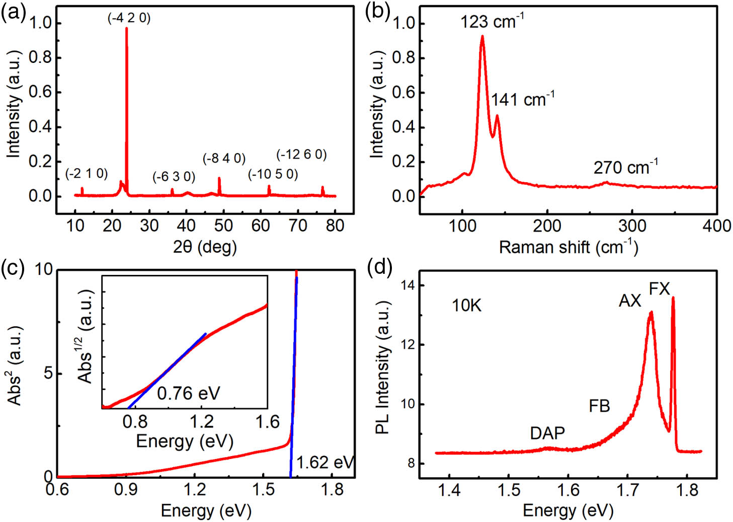
Single-crystal GaTe was grown by the Bridgman method. The symmetry of GaTe bulk crystal can be depicted by the (C2/m) space group. It includes one twofold rotation axis perpendicular to a mirror plane, which is equivalent to a point inversion when applied consecutively in GaTe. The () planes are preferential for cleavage, since these planes are only bonded to each other by the van der Waals interaction. A cleaved sample of and with a thickness of 0.24 mm was prepared using a razor blade. The () surfaces of the sample were mirror-like and needed no further cleaning, polishing, or etching treatment. Figure 1(a) shows the X-ray diffraction (XRD) spectrum with six distinct peaks corresponding to the (), (), (), (), (), and () crystal planes. The Raman scattering spectrum of GaTe measured at room temperature, by a Renishaw inVia Micro-Analysis System with a laser of 785 nm wavelength, is shown in Fig. 1(b). The peaks at and were assigned with the lattice vibration of the Ag-type symmetry, matching our previous report [28]. Figure 1(c) demonstrates UV-Vis-NIR absorption spectra from 0.6 to 1.8 eV. The linear extrapolation of the square of absorbance reveals a 1.62 eV direct band-to-band bandgap. Absorption of photons with energies below the band edge can be observed. The inset of Fig. 1(c) shows the linear relation between the square root of absorption over energy characteristic, revealing an indirect transition at about 0.76 eV. This absorption edge cannot be attributed to the formation of the common oxide-decomposition products, such as (3.8 eV) and (4.9 eV) [29]. The photoluminescence (PL) spectroscopy was carried out at 10 K, with a Jobin Yvon spectrophotometer at a 488 nm laser excitation. According to our previous work [28] and established energy levels in PL spectra of GaTe single crystals [30], the strong sharp peak centered at 1.78 eV represents the free excitonic (FX) emission. The peak marked with AX corresponds to the acceptor excitonic transition. The peaks manifest at high crystalline quality. The peak centered at 1.56 eV corresponds to donor-acceptor pair (DAP) transition. The weak DAP bands and the sharp and strong FX bands indicate high perfection of the crystal structure, with low defect concentrations [28].
Figure 1.Characterization of the GaTe crystal by (a) an XRD spectrum; (b) a Raman spectrum with a laser wavelength of 785 nm; (c) optical absorption spectra, with the excitonic absorption observed around 1.62 eV. Inset in (c) shows square root of the absorption as a function of energy, where the linear extrapolation reveals an optical bandgap of 0.76 eV, associated with an indirect bandgap; (d) PL spectrum of GaTe at 10 K under 488 nm laser excitation.
THz radiation from a GaTe crystal has been investigated at room temperature. The used THz time domain emission spectroscopy system in transmission configuration is illustrated in Fig. 2(a). A regeneratively amplified Ti:sapphire laser system (Spectra-Physics, Spitfire) generates laser pulses with a wavelength of 800 nm and a duration of 35 fs, at a repetition frequency of 1 kHz. The laser beam is divided by a beam splitter into two parts, namely, the pump beam and the probe beam. The pump beam (3 mm in diameter) is focused onto the GaTe sample. The polarization states of the pump beam can be varied with a half-wave plate (HWP). The THz radiation is collected via two off-axis parabolic mirrors and is afterwards focused collinearly onto a 2 mm thick (110) zinc telluride (ZnTe) crystal together with the probe beam. The probe beam is s-polarized by a Glan–Taylor prism (GTP), and the power is fixed at 1.2 mW. THz radiation is p-polarized via a wire-grid polarizer (WGP). An autobalanced detector combined with a quarter-wave plate and a Wollaston prism are used to detect the differential intensity of beams, which is proportional to the THz signal. The ZnTe crystal is rotated to the optimized crystal direction. A Teflon/high resistance silicon wafer () is used to block the residual 800 nm pump beam and to eliminate the THz signal from air ionization. The silicon plate can totally block the residual laser, and the THz signal can pass through the plate. The polarization of the pump beam and the polarization of THz waves [ horizontal polarization, vertical polarization in Fig. 2(b)] are demonstrated in Fig. 2(b), with XYZ representing the orthonormal Cartesian laboratory coordinate system (CS). The XY plane is the () sample surface plane. The polarization of the pump beam and the incident angle (angle between pump beam and Z direction) are defined by and , respectively. In this way the pump beam is -polarized () when , and the pump beam is -polarized () when .
Figure 2.Experimental setup of the THz emission spectroscopy system used. (a) Schematic illustration. GTP, Glan–Taylor prism; HWP, half-wave plate; WGP, wire-grid polarizer. (b) Sample in transmission configuration. XYZ represents the Cartesian laboratory CS.
Likewise, represents that the THz electric field is parallel to the XZ plane. represents normal incidence of the pump beam. Furthermore, the azimuthal angle of the GaTe sample can be varied by simply rotating the sample along the Z direction.
3. RESULTS AND DISCUSSION
A. THz Radiation
The component of the generated THz electric field can be extracted with a perpendicularly aligned WGP in the optical path. Figure 3 shows a typical time domain THz spectrum and its Fourier-transformed spectrum of GaTe, at a pump fluence of . The central frequency of the spectrum is approximately 0.68 THz, and the bandwidth is 2.2 THz (from 0.3 to 2.5 THz). The absolute values of the THz electric field can be calculated according to the current measurement from the lock-in amplifier as follows [31]: Here, the nonzero electro-optic coefficient of ZnTe is 3.9 pm/V, the refractive index of ZnTe in the infrared region is about 2.8, is the speed of light in vacuum, is the circular frequency, and is the length of the crystal of 2 mm. In the experiment, the probe current μ, with a peak amplitude of . Therefore, we can calculate the peak value of the THz electric field for GaTe to be , which is about 9.4% of the value generated from state-of-the-art InAs [15]. According to the previous demonstration of GaTe [21], this value could be enhanced by adjusting the spot size and excitation wavelength on the samples.
Figure 3.Typical THz waveform in (a) time domain and (b) frequency domain generated from layered GaTe.
We can change the pump polarization and incident angle by using an HWP and rotating the sample holder, respectively. As shown in Figs. 4(a) and 4(b), under normal incidence (), THz radiation from p-polarized and s-polarized excitation ( and ) is not identical; the incident angle is 40°; in amplitude, they show reversed polarities. In contrast, when the incident angle is 40°, the THz radiation under is about 3 times stronger than that from , and the polarities are in-phase. Since the THz radiation is generated at a photon energy of the laser beam, which is lower than the bandgap of a centrosymmetric GaTe crystal, the mechanism of THz generation from the GaTe crystal needs further investigation.
Figure 4.X component of the generated THz waveforms from GaTe under p-polarized (Pin) and s-polarized (Sin) excitation with (a) 0° and (b) 40° incident angle; (c) X component of generated THz waveforms from GaTe under 40°, , 0° incidences; (d) peak-to-valley values of THz pulses from GaTe as a function of incident angle.
Generally, there are two competing mechanisms for broadband THz generation in semiconductor materials, i.e., instantaneous material polarization (optical rectification, OR) and ultrafast transient of charged carriers (photocurrent surge, PS). This can be expressed as follows: where the first term on the right side is the contribution of OR and the second term represents PS. The OR contribution to the THz electric field is proportional to the second-order derivative of nonlinear dielectric polarization to time . The nonlinear polarization depends on the crystal symmetry and shows an azimuthal angle dependence. The contribution of PS to is the derivative of the photocurrent density with respect to time . It commonly shows no dependence on the symmetry of the crystal and has a linear relation with the intrinsic or extrinsic electric field.
Both of these two mechanisms play dominant roles in the generation of broadband THz pulses. Conventional OR was among the first nonlinear optical effects discovered [32]. It refers to the generation of dc electric polarization by applying an intense optical beam to a nonlinear medium, such as ZnTe [33], InP [34], or CdTe [35]. THz emission via nonlinear OR strongly depends on the pump polarization and the azimuthal angle of the crystal, as dictated by the form of the second-order nonlinear susceptibility tensor .
Generally, THz radiation polarity is barely influenced by the incident polarization from the PS mechanism, either by intrinsic electric field or by extrinsic electric field. The THz polarity from the surface depletion field is dictated by the doping type, rather than the excitation polarization in semiconductors, while the THz polarity from the photo-Dember effect induced field is determined by the discrepant mobility between electrons and holes. However, THz polarity generated from GaTe is definitely influenced by the pump polarization. Similar to graphene [36] and 2H-[14,15], the polarity reversal under different excitation polarization stems from the nonlinear process. So, the primary mechanism of THz generation of GaTe is the OR effect.
To further confirm this speculation, we show THz radiation from GaTe under , 0°, and 40° incidences in Fig. 4(c). The peak amplitudes of the THz radiation under -incidence and 40°-incidence are basically identical, but the polarities are reversed. The value of the THz amplitude is over 5 times larger than that under normal incidence. At the oblique incident angle, such as 40° incidence, GaTe demonstrates increscent THz radiation. The polarities of the THz waveforms of the GaTe crystal will reverse in polarity when the angle is switched from positive to negative direction, as shown in Fig. 4(d), similar to that of (100) GaAs [14]. However, (100) GaAs shows no THz signal, as there is no OR contribution under normal incidence. On the contrary, GaTe shows obvious THz emission even under normal incidence, which suggests that OR may contribute to the THz radiation in GaTe. Similar to 2H-MoS2[15], reorganization of atoms on the surface breaks the bulk inversion symmetry [25,26]. The results of combined scanning tunneling microscopy and spectroscopy (STM/STS) and low energy electron diffraction (LEED) study of the GaTe cleavage surface indicate the presence of different atomic structures of bulk GaTe and its surface. So, the OR effect may be an essential effect in THz generation from GaTe, as the hexagonal structure at the surface is noncentrosymmetric and holds a P-6m2 crystal structure.
C. Analysis of the OR Effect
To further confirm THz radiation from the OR effect, its dependence on the azimuthal angle of the GaTe sample and the pump polarization angle is investigated. In the experiments, the excitation laser beam is always p-polarized. We determined the dependence of peak-to-valley values of the components as a function of azimuthal angle , as shown in Fig. 5(a). The THz signal as a function of the azimuthal angle under normal incidence presents three peaks, indicating a distorted threefold symmetry.
Figure 5.THz radiation peak-valley amplitude as a function of (a) azimuthal angle and (b) pump polarization angle under normal incidence. The experimental data and the fitting according to the OR and PS model are depicted by black squares and solid lines, respectively.
We proposed a theoretical model to describe the THz generation process. The emitted THz radiation, generated from the sample surface, transmits the sample and radiates out from the opposite surface of the crystal. The transmitted beam leaves the sample with the incident angle, as indicated by Snell’s law [37]Here, and are the refraction angles between the surface of the crystal and the propagating direction for the incident laser beam and the generated THz radiation. Analogously, and are the refractive indices of the sample for the incident laser beam and the generated THz radiation.
The THz radiation from the OR effect can be calculated using the following equation [37]: where and are and Z components of the nonlinear dielectric polarization. is the refraction angle of the generated THz wave within the sample, which is determined by Snell’s law. The prerequisite of invariance of to the crystal symmetry of GaTe eliminates most of its components (see Appendix A, Part 1). Applying the invariant susceptibility tensor and inserting the resulting dielectric polarization to the generated THz radiation in Eq. (4), results in representing the azimuthal angular dependence of due to OR in GaTe.
The observed experimental results in Fig. 5(a) do not agree with the simple 3 dependence from Eq. (5). However, there seems to be a cosine perturbing the threefold symmetry, suggested by the OR model. We speculate that the cosine contribution originating from the PS at the crystal surface, due to its noncubic electric properties, results in unidirectional charge carrier diffusion because the PS contribution perpendicular to the crystal surface cannot be detected under normal incidence. Besides, the THz amplitude from the PS within the crystal surface should not change with the pump polarization. To confirm that the cosinoidal contribution actually arises from the PS within the crystal surface, the dependence of the THz amplitude on the polarization of the pump beam is depicted in Fig. 5(b). The generated THz amplitude as a function of the incident polarization angle can be expressed as where is the fitting constant, which is derived from the previous calculation. The dependence on the pump polarization angle is dominated by OR, which complies with Eq. (6). And the amplitude of THz radiation from GaTe presents a large shift of the value, shown in Fig. 5(b). The shift shows no change when pump polarization changes from 0° to 360°, which indicates that the shift is coming from the photocurrent within the surface.
The noncubic anisotropy of the electric properties can be confirmed by the resistivity characterization. The resistivity of several GaTe samples was measured by the van der Pauw method. The resistivity can be calculated by where is the current applied between contacts and on one side of the sample surface, is the voltage measured between contacts and on opposite sides of the sample surface, and is the sample thickness. A high-resistivity anisotropy was revealed by this measurement. We also confirmed the reproducibility of this anisotropy by measuring three different samples, as shown in Table 1. These results indicate a high noncubic mobility anisotropy within the surface layer and a unidirectional diffusion of photogenerated carriers there, which dominates part of THz generation.
Sample
t mm
ρ12
ρ34
Average
ρ23
ρ14
Average
(Ω·cm)
1
0.21
134
108
121
1785
1259
1522
2
0.53
103
105
104
1430
1448
1439
3
0.17
187
187
187
1465
1449
1457
Table 1. Resistivity Anisotropy of Bulk GaTe Surface
As discussed earlier, OR is likely the dominant mechanism for the THz generation in GaTe crystals, in which the phase matching is negligible due to the nanometer-level interaction depth. It is worth noting that PS perpendicular to the layer plane could be still one of the possible mechanisms, because the generated THz radiation along the surface normal cannot be detected in such an experimental configuration. Therefore, we set the incident angle of the p-polarized () pump beam to be 40°. Its dependence on the azimuthal angle and pump polarization angle is shown in Fig. 6. In contrast to the results from the normal incidence, the azimuthal angle dependence shows perfect threefold symmetry, while the dependence on pump polarization angle is still twofold symmetrical. The THz amplitude of the dependence on the azimuthal angle is about 0.6 times of that in the normal incidence case, which is consistent with the theoretical calculations. After taking the Fresnel reflections at the crystal/air interface into consideration, the data in Fig. 6(b) can be well fitted [see Appendix A, Part 1, Eq. (A15)]. However, the amplitudes of the THz signal are largely negative, as shown in Figs. 6(a) and 6(b). This might be attributed to the generation of the PS perpendicular to the surface. The PS can originate from the drift of the photogenerated carriers under a surface electric field and the photo-Dember effect. The photo-Dember effect is usually caused by the difference in diffusion coefficients for electrons and holes. Such an effect can also be induced by a structural asymmetry [38]. The polarity reversal of the THz amplitude (THz amplitude sign change) when changing incident angle [Fig. 4(d)] is also evidence of photoinduced currents propagating in a direction perpendicular to the surface, similar to (100) GaAs and (100) InAs crystals [39]. To further verify this, we do the theoretical calculation of the THz amplitude as a function of incident angle of the laser beam, as shown in Appendix A, Part 2, Eqs. (A16) and (A17). We can estimate the ratio of the nonlinear contribution to the total THz radiation using the data in Figs. 5 and 6. The contribution from OR is more than 90% under normal incidence and decreases to approximately 23% under 40° incidence.
Figure 6.THz peak-valley amplitude as a function of (a) azimuthal angle and (b) pump polarization angle under 40° incident angle. The experimental data and the fitting according to the OR and PS model are depicted by black squares and solid lines, respectively.
The pump energy fluence depends on THz peak-to-valley value in the transmission configuration. In our experiment, we set the pump beam to be p-polarized and the azimuthal angle to be 0°. As shown in Fig. 7, the THz radiation amplitude increases with the increase of the pump influence. At normal incidence, the THz amplitude is expected to be linearly proportional to the pump fluence, since it depends quadratically on the incident electric field within the OR process [Eq. (4)]. The deviation from the linear function accounts for the PS contribution of the THz amplitude, which is proportional to the square root of the pump fluence. At 40° incidence, the contribution of the linear part diminishes, and the square root contribution is dominant. The results shown in Fig. 7 suggest that the dominant THz generation mechanism is changed from OR to PS when the incident angle changes from 0° to 40° as the curve changes from linear to square root.
Figure 7.Pump fluence dependence of THz peak-to-valley amplitude generated from GaTe at (a) 0° and (b) 40° incident angle.
We observed THz radiation ranging from 0.3 to 2.5 THz generated from a layered GaTe bulk crystal by THz emission spectroscopy in a transmission configuration. The THz radiation waveforms under different polarization states and different pump incident angles of the pump beam indicate a second-order nonlinear THz generation process. The calculated data—based on the theoretical analysis of the interaction between incident electric field and the material—fit well with the experimental results. In addition, we also demonstrated the unidirectional diffusion of carriers within the layer planes of GaTe, which was supported by a resistivity measurement based on the van der Pauw method. The induced THz radiation by the PS perpendicular to the surface plane is confirmed by changing the incident angle of pump beam from to 40°. Based on our analysis, the evolution of the contribution from OR is decreasing from 90% at normal incidence to 23% at 40° incidence. The investigation does not only clarify the mechanism of THz generation of bulk GaTe layered semiconductor, but also proves that THz emission spectroscopy is a sensitive nondestructive tool for characterizing surfaces and interlayer properties.
Acknowledgment
Acknowledgment. We thank Prof. Xinlong Xu and Dr. Yuanyuan Huang from the Institute of Photonics & Photon-Technology, Northwest University, Xi’an for helping with the THz measurements.
[7] M. Yamashita, C. Otani, H. Okuzaki, M. Shimizu. Nondestructive measurement of carrier mobility in conductive polymer PEDOT: PSS using terahertz and infrared spectroscopy. 30th URSI General Assembly and Scientific Symposium, 1-4(2011).
[18] K. C. Mandal, R. M. Krishna, T. C. Hayes, P. G. Muzykov, S. Das, T. S. Sudarshan, S. Ma. Layered GaTe crystals for radiation detectors. IEEE Nuclear Science Symposium & Medical Imaging Conference, 3719-3724(2010).