
Shiyin Cao, Liping Hou, Qifa Wang, Chenyang Li, Weixing Yu, Xuetao Gan, Kaihui Liu, Malin Premaratne, Fajun Xiao, Jianlin Zhao. Augmenting photoluminescence of monolayer MoS2 using high order modes in a metal dimer-on-film nanocavity[J]. Photonics Research, 2021, 9(4): 501
- Photonics Research
- Vol. 9, Issue 4, 501 (2021)
Abstract
1. INTRODUCTION
Plasmonic nanostructures show unprecedented ability to confine light in subwavelength volume due to the surface plasmons they support. This peculiar feature is responsible for a plethora of enhanced optical processes, including surface-enhanced Raman scattering [1], photoemission [2], nonlinear optics [3], and nanolasing [4,5]. To achieve a strong light–matter interaction in aforementioned phenomena, it is essential to carefully mold plasmonic nanostructures. For example, optimizing the patterned metallic structures can align the plasmon resonances with the absorption and/or emission bands of the monolayer atop that produce strong and well-manipulated plasmon–exciton interactions and promise high-efficiency and ultrafast optoelectronic applications [6–9]. Also, recently, it has been demonstrated that the Anderson localization resulting from an increasing of the disorder in silver nanoarrays is possible to further squeeze the localized surface plasmon, giving rise to a substantially enhanced photoluminescence (PL) of dye molecules [10]. With the advance of nanofabrication and colloidal approaches, plasmonic nanostructures with a small feature/gap size can be readily prepared as exemplified by the crescent-ring [11], bowtie antenna [12], and Au nanosphere dimer [13], allowing for confining light down to tens of nanometers to probe novel light–mater interactions. However, further scaling the light confinement volume requires controlling the structure feature/gap size with nanometer accuracy, presenting a tremendous challenge even for state-of-the-art lithographic and colloidal methods. A promising solution is integrating the sharp metallic protrusion into a scanning probe microscopy, such as a tip-enhanced spectroscopy (TES) configuration. This enables an extreme confinement of light with the nanometric mode volume, rendering a PL enhancement of three orders for the monolayer [14].
Alternatively, the rapidly growing metal particle-on-film nanocavity [15–19], composed of a closely spaced nanoparticle and metal film, provides an up-and-coming solution to squeeze light in the true nanometer or even subnanometer region. For example, using thin film deposition technology and the bottom-up process, the spacer between the Au nanosphere and metal film can be well tuned with the precision of a few angstroms, yielding a field enhancement factor of over [15]. This intriguing property not only facilitates the observations of exciting phenomena including strong coupling [20–22] and quantum tunneling [23], but also enables fascinating applications in hyper-spectral imaging [24], nanoscale sensing [25], and switching [26]. More importantly, benefitting from the bottom-up process, it is much more convenient to precisely place the active media (e.g., molecules [27], quantum dots [28], and two-dimensional materials [29]) in the nanogaps, making the single-molecule-level light–matter interactions possible.
Monolayer molybdenum disulfide () is an appealing building block for future nanophotonics and optoelectronics devices relying on its intriguing optical properties [30,31]. However, for practical application, it is highly needed to enhance its intrinsically low absorption [32] and small PL quantum yield [33]. Recently, Au nanosphere dimer-on-film nanocavities (DoFNs) have been demonstrated to be the ideal platform for realizing strong light–matter interactions, owing to their wealth of plasmon modes resulting from particle–particle and particle–film couplings [34,35]. Recently, a large number of experimental studies have paid attention to PL enhancement using the dipole or coupled dipole modes of DoFNs [18,36]. However, relying on high order modes is scarce, as their dark-mode nature possesses a much stronger electric field enhancement. In this work, we fabricate Au nanosphere DoFNs with a single-particle diameter of 140 nm. The polarization-resolved scattering spectra of DoFNs reveal the film-coupled bonding quadrupole modes. These modes allow us to simultaneously boost the absorption and emission processes of the monolayer , achieving a 1350-fold PL enhancement.
Sign up for Photonics Research TOC. Get the latest issue of Photonics Research delivered right to you!Sign up now
2. EXPERIMENTAL AND SIMULATION DETAILS
The Au nanosphere DoFNs were fabricated using the bottom-up self-assembly technique. Specifically, a 50-nm-thick Au substrate with atomic flatness was prepared via thermal evaporation at a deposition rate of 1 Å/s (1 Å = 0.1 nm) followed by a template-stripping method [37]. Then, to avoid PL quenching, an spacer layer with a thickness of 6 nm was deposited on the Au substrate by the atomic layer deposition technique. The monolayer was mechanically exfoliated from bulk crystal (HQ-graphene, Inc.), and then deterministically transferred onto the layer with the help of a polydimethylsiloxane gel-film. Finally, 140-nm-diameter Au nanospheres (Nanoseedz, Inc.), coated with a 2 nm cetyltrimethylammonium bromide surfactant polymer, were drop-cast on the monolayer and blow-dried in air for seconds to form nanosphere dimers.
In our measurement, the dark-field images and scattering spectra of the DoFNs are characterized using a home-built dark-field confocal microscope [38], where a polarization-controlled white light from a halogen lamp is obliquely illuminated on the sample through a objective (Mitutoyo, NA 0.4) at an incident angle of 60°. The scattering light is collected with an upright objective (Nikon NA 0.6), and then recorded as the dark image and scattering spectrum by a CCD camera and an imaging spectrometer (Andor Shamrock SR-500i), respectively. The PL measurement was carried out on the same confocal microscope. A He–Ne laser beam (wavelength at 633 nm) with a power of is focused on the sample through a objective (Leica, NA 0.9). The diameter of the focused excitation beam is estimated to be in the sample plane. The backscattered PL emission is collected by the same objective. After passing through a long-pass filter, the collected emission is delivered to the spectrometer for spectral analysis. Notice that the dimer with a separation at least 2 μm away from other nanosphere clusters and the edge was deliberately selected by spatially filtering optical signals through a pinhole, to avoid the unwanted scattering and PL contributions.
The optical responses of a plasmonic nanocavity are calculated by a full-wave simulation based on the finite element method (FEM). The structural configurations are modeled as the true values of the fabricated system. The permittivity of Au is taken from the experimental data of Johnson and Christy [39]. The refractive index of the layer is taken as a constant of 1.5. The permittivity of monolayer is modeled by the experimental data of Jung
The quantum yield enhancement of the nanocavity coupled was calculated with the finite-difference time domain method, where the monolayer was set as a monochromatic dipole with a horizontal orientation. We calculated the dyadic Green’s function of the hybrid system by varying the dipole position on a discrete grid () beneath the dimer [42]. The radiative and non-radiative decay rates were obtained by integrating the power radiated out of the hybrid system and absorbed by the DoFN, respectively.
3. RESULTS AND DISCUSSION
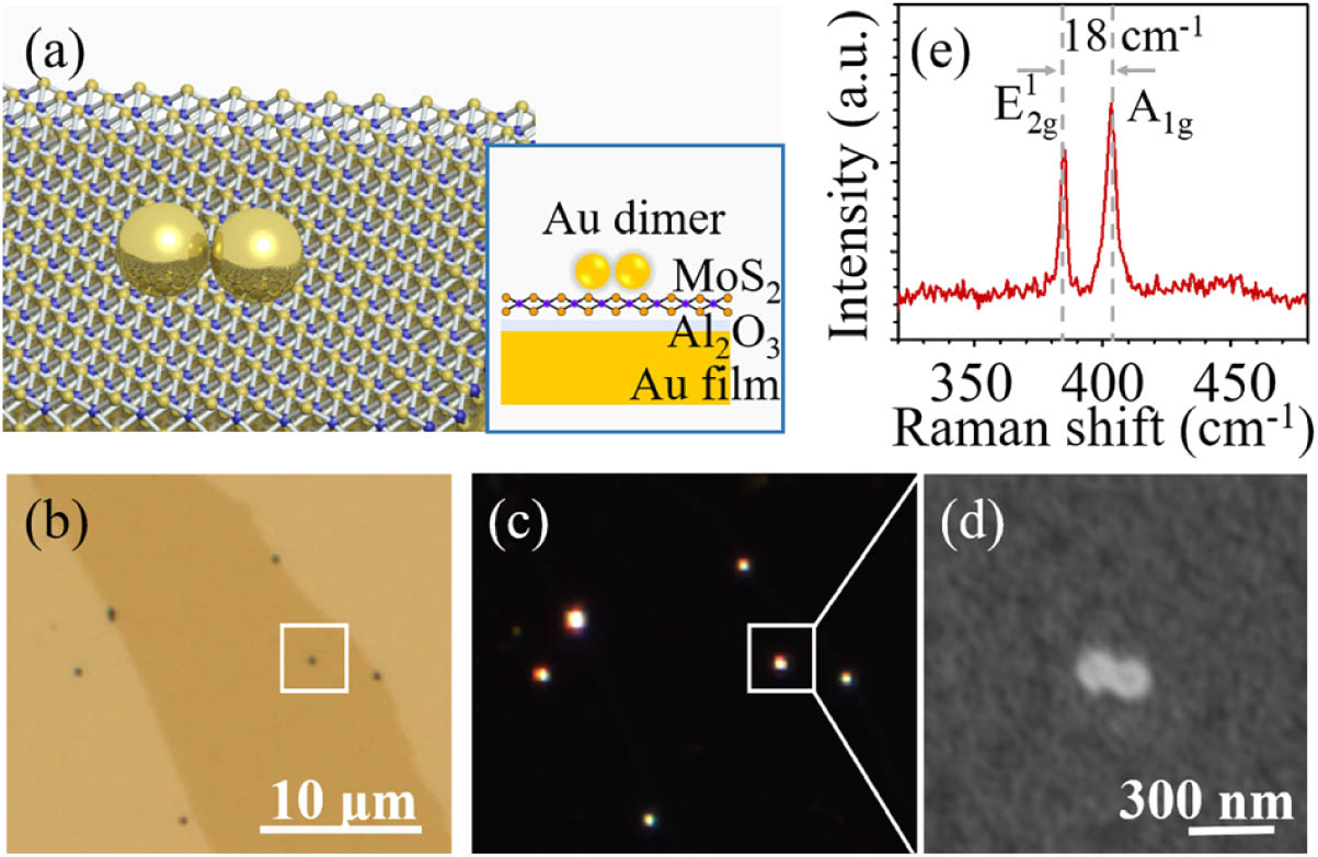
Figure 1.(a) Schematic of Au nanosphere dimer-on-film nanocavity (DoFN) composed of the Au nanosphere dimer and Au film spaced by the monolayer
![]()
Figure 2.(a)–(d) Scattering spectra of Au nanosphere DoFNs illuminated with two typical wave vectors and polarizations shown in the insets of left panels. Here, the left and right panels are for the experiment and simulation results, respectively.
![]()
Figure 3.(a)–(f) Charge distributions (upper panels) and electric field enhancement maps (lower panels) of modes I–VI shown in Fig.
![]()
Figure 4.(a) Photoluminescence (PL) spectra of
The difference in enhancement factors between two orthogonal polarizations can be attributed to the plasmonic modes participating in PL enhancement. When the polarization is along the dimer axis, the tightly focused PL excitation can be decomposed into the -polarized beam of configuration 1 and -polarized beam of configuration 2. Therefore, it excites modes I, V, and VI to enhance the PL of . For the polarization perpendicular to the dimer axis, the PL excitation can be regarded as the -polarized beam of configuration 1 and -polarized beam of configuration 2, which excite modes II–IV to boost the PL. As seen in the lower panels of Fig. 3, modes I, V, and VI produce overall stronger field enhancement than modes II–IV. Additionally, modes I and V are more in resonance with the PL excitation, eventually contributing to a larger PL enhancement factor when the polarization is along the dimer axis. Thus, we evaluate the PL enhancement for two orthogonal polarizations by [42]
4. CONCLUSION
In summary, we have fabricated a particle-on-film nanocavity composed of the Au nanosphere dimer and ultra-smooth Au film. The polarization-resolved scattering spectra uncover a high order plasmon mode of the nanocavity. Further full-wave simulations confirm these modes are attributed to two longitudinal bonding quadrupoles of the dimer coupled with their images in the Au film. By integrating the monolayer into the nanocavity, we demonstrate these high order modes can enhance the PL intensity of through boosting both the absorption and emission processes, leading to a 1350-fold enhancement factor. Our results pave the way for exploiting high order plasmon modes to enhance light–matter interactions at the nanoscale and have potential applications in future optoelectronics and nanophotonics devices such as light-emitting diodes, photovoltaics, and photodetectors.
Acknowledgment
Acknowledgment. The authors acknowledge the SEM measurements by the Analytical and Testing Center of Northwestern Polytechnical University.
References
[10] Y. Zhu, H. Jing, R.-W. Peng, C.-Y. Li, J. He, B. Xiong, M. Wang. Realizing Anderson localization of surface plasmon polaritons and enhancing their interactions with excitons in 2D disordered nanostructures. Appl. Phys. Lett., 116, 201106(2020).

Set citation alerts for the article
Please enter your email address
© Copyright 2018-2021 | Chinese Laser Press. All Rights Reserved 沪ICP备15018463号-20