
Wang Yu, Zhou Yanping, Li Maolin, Zuo Chao, Yang Bingjun. ICP Etching Process of GaAs/AlGaAs for Vertical-Cavity Surface-Emitting Lasers[J]. Chinese Journal of Lasers, 2020, 47(4): 401005
- Chinese Journal of Lasers
- Vol. 47, Issue 4, 401005 (2020)
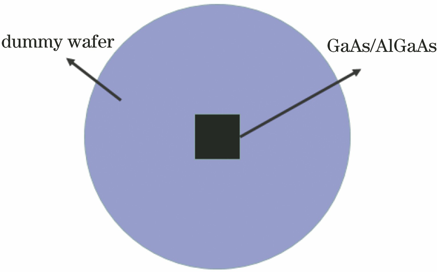
Fig. 1. Schematic of GaAs/AlGaAs sample wafer and Si chip

Fig. 2. Schematic of etching process
Fig. 3. Etching rate versus ICP antenna power
Fig. 4. SEM images of GaAs/AlGaAs etching profile for different ICP antenna powers. (a) 800 W; (b) 1400 W; (c) 1600 W
Fig. 5. Etching rate versus RF bias power
Fig. 6. SEM images of GaAs/AlGaAs etching profile for different RF bias powers. (a) 300 W; (b) 500 W; (c) 600 W
Fig. 7. Curves of etching rate with cavity pressure
Fig. 8. SEM images of GaAs/AlGaAs etching profile for different cavity pressures. (a) 0.8 Pa; (b) 1.2 Pa; (c) 1.4 Pa
Fig. 9. SEM image of the final etching result. (a) Sample table; (b) sample profile


Set citation alerts for the article
Please enter your email address

© Copyright 2018-2021 | Chinese Laser Press. All Rights Reserved 沪ICP备15018463号-20