• Photonics Research
  • Vol. 11, Issue 10, 1694 (2023)
Mauro David1, Davide Disnan2, Elena Arigliani1, Anna Lardschneider1, Georg Marschick1, Hanh T. Hoang1, Hermann Detz1、3, Bernhard Lendl4, Ulrich Schmid2, Gottfried Strasser1, and Borislav Hinkov1、*
Author Affiliations
  • 1Institute of Solid State Electronics and Center for Micro- and Nanostructures, TU Wien, Vienna, Austria
  • 2Institute of Sensor and Actuator Systems, TU Wien, Vienna, Austria
  • 3Central European Institute of Technology, Brno University of Technology, Brno, Czech Republic
  • 4Institute of Chemical Technologies and Analytics, Vienna, Austria
  • show less
    DOI: 10.1364/PRJ.495729 Cite this Article Set citation alerts
    Mauro David, Davide Disnan, Elena Arigliani, Anna Lardschneider, Georg Marschick, Hanh T. Hoang, Hermann Detz, Bernhard Lendl, Ulrich Schmid, Gottfried Strasser, Borislav Hinkov, "Advanced mid-infrared plasmonic waveguides for on-chip integrated photonics," Photonics Res. 11, 1694 (2023) Copy Citation Text show less
    (a) Cross section of the DLSPP waveguide. (b) |Ey| 2D-field profile of the TM00 SPP mode for a 3.6 μm×3.6 μm DLSPP waveguide at λ=9.26 μm. (c) Top view of the 3D simulation of the waveguide.
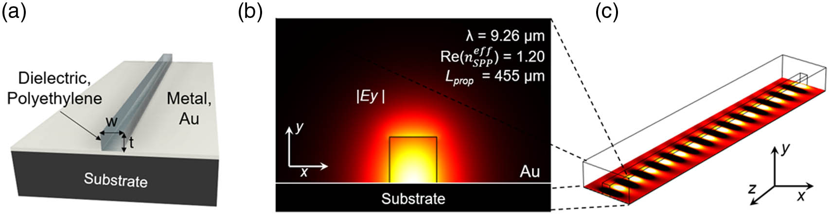
    Fig. 1. (a) Cross section of the DLSPP waveguide. (b) |Ey| 2D-field profile of the TM00 SPP mode for a 3.6  μm×3.6  μm DLSPP waveguide at λ=9.26  μm. (c) Top view of the 3D simulation of the waveguide.
    (a) Mode effective index Neff for different ridge dimensions. (b) Propagation length Lp for different ridge dimensions.
    Fig. 2. (a) Mode effective index Neff for different ridge dimensions. (b) Propagation length Lp for different ridge dimensions.
    (a) Influence of the PE ridge geometries on the effective mode area (Aeff/A0). (b) Comparison of the transmission (Ib/Ia) of a 90° PE DLSPP waveguide bend (cross section of 3.6 μm×3.6 μm) at λ=9.26 μm and a PMMA DLSPP waveguide (cross section of 600 nm×600 nm) at λ=1.55 μm as a function of its normalized radius (R/λ). Inset: 3D modeling of the PE waveguide mode.
    Fig. 3. (a) Influence of the PE ridge geometries on the effective mode area (Aeff/A0). (b) Comparison of the transmission (Ib/Ia) of a 90° PE DLSPP waveguide bend (cross section of 3.6  μm×3.6  μm) at λ=9.26  μm and a PMMA DLSPP waveguide (cross section of 600  nm×600  nm) at λ=1.55  μm as a function of its normalized radius (R/λ). Inset: 3D modeling of the PE waveguide mode.
    Schematic flow chart of the chip fabrication process, (a) using an Au hard mask and (b) using a Cr hard mask.
    Fig. 4. Schematic flow chart of the chip fabrication process, (a) using an Au hard mask and (b) using a Cr hard mask.
    Typical AFM image of the fabricated PE films right after spin coating. rms area roughness amounts to Sq=10.4 nm.
    Fig. 5. Typical AFM image of the fabricated PE films right after spin coating. rms area roughness amounts to Sq=10.4  nm.
    Scanning electron microscope (SEM) image of a DLSPP PE-waveguide structure. (a) Plasmonic waveguide and (b) Closeup of the 8 µm wide and 1 µm high PE stripe.
    Fig. 6. Scanning electron microscope (SEM) image of a DLSPP PE-waveguide structure. (a) Plasmonic waveguide and (b) Closeup of the 8 µm wide and 1 µm high PE stripe.
    (a) Summary of measured data in terms of waveguide losses (left) and coupling losses (right) extracted from the effective cutback method. The square points represent the losses extracted with the cutback method per each waveguide width. Dashed lines represent the exponential fit of the results obtained from the simulations. (b) Mode-profile simulations of the fabricated DLSPP waveguides, indicating their respective width (w) and thickness (t) measured with a profilometer.
    Fig. 7. (a) Summary of measured data in terms of waveguide losses (left) and coupling losses (right) extracted from the effective cutback method. The square points represent the losses extracted with the cutback method per each waveguide width. Dashed lines represent the exponential fit of the results obtained from the simulations. (b) Mode-profile simulations of the fabricated DLSPP waveguides, indicating their respective width (w) and thickness (t) measured with a profilometer.
    (a) SEM images of the S-bend structures (width w=5 μm and thickness t=3 μm) with an offset of d=75 μm. (b) S-bend transmission dependence on the offset distance between the two arms (Sections A and B) obtained by numerical modeling and measurements. The inset shows the top view of the 3D simulations for offsets of d=24 μm and d=96 μm.
    Fig. 8. (a) SEM images of the S-bend structures (width w=5  μm and thickness t=3  μm) with an offset of d=75  μm. (b) S-bend transmission dependence on the offset distance between the two arms (Sections A and B) obtained by numerical modeling and measurements. The inset shows the top view of the 3D simulations for offsets of d=24  μm and d=96  μm.
    Waveguide PlatformWavelength (µm)Propagation Length (mm)Attenuation (dB/mm)Mode Guiding CapabilitiesReferences
    60 µm wide gold stripe7.51.82.41No[63]c
    15 µm wide and 200 nm thick SiNx stripe on Au6.52–42.1–1.1No[19]a
    15 µm wide and 200 nm thick SiNx stripe on Au6.11.72.55No[6]a,b
    6.21.82.41
    9 µm wide and 300 nm thick Ge stripe on Au9.120.6456.73No[45]c
    5 µm wide and 450 nm thick PE stripe on Au9.2622.5NoThis paper
    5 µm wide and 3 µm thick PE ridge on Au9.260.3111–3 dB (90° bend with 26 µm radius)YesThis paper
    Table 1. Comparison of Mid-IR Plasmonic Waveguide Platforms
    Offset (µm)Simulation (dB)S-bend Losses (dB)Scattering (defects) (dB)Band Losses (dB)
    502.303.180.881.31
    753.455.221.772.33
    Table 2. Simulated and Measured S-bend Losses (for a 106 µm Long S Bend)a
    Mauro David, Davide Disnan, Elena Arigliani, Anna Lardschneider, Georg Marschick, Hanh T. Hoang, Hermann Detz, Bernhard Lendl, Ulrich Schmid, Gottfried Strasser, Borislav Hinkov, "Advanced mid-infrared plasmonic waveguides for on-chip integrated photonics," Photonics Res. 11, 1694 (2023)
    Download Citation