• High Power Laser Science and Engineering
  • Vol. 4, Issue 1, 01000e11 (2016)
Jan Vanda1, Jan ˇSevˇcík1, Egidijus Pupka2, Mindaugas ˇS ˇciuka2, Andrius Melninkaitis3, Martin Divok′y1, Venkatesan Jambunathan1, Stefano Bonora1、4, V′aclav ˇSkoda5, Antonio Lucianetti1, Danijela Rostohar1, Tomas Mocek1, and Valdas Sirutkaitis3
Author Affiliations
  • 1Hilase, Institute of Physics AS CR, Za Radnicí 828, 252 41 Dolní Bˇreˇzany, Czech Republic
  • 2LIDARIS Ltd., Saul˙etekio Al. 10, LT-10223, Vilnius, Lithuania
  • 3Laser Research Center, Vilnius University, Sauletekio Al. 10, LT-10223 Vilnius, Lithuania
  • 4LUXOR Laboratory, CNR IFN, Via Trasea 7, 35131, Padova, Italy
  • 5Crytur Ltd., Palackeho 175, 511 01 Turnov, Czech Republic
  • show less
    DOI: 10.1017/hpl.2016.11 Cite this Article Set citation alerts
    Jan Vanda, Jan ˇSevˇcík, Egidijus Pupka, Mindaugas ˇS ˇciuka, Andrius Melninkaitis, Martin Divok′y, Venkatesan Jambunathan, Stefano Bonora, V′aclav ˇSkoda, Antonio Lucianetti, Danijela Rostohar, Tomas Mocek, Valdas Sirutkaitis. Comparative LIDT measurements of optical components for high-energy HiLASE lasers[J]. High Power Laser Science and Engineering, 2016, 4(1): 01000e11 Copy Citation Text show less
    Schematics of laser systems developed at HiLASE project and respective LBDSs.
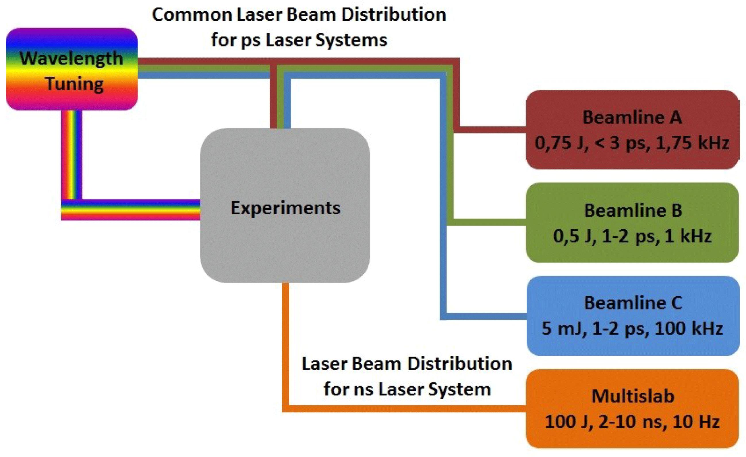
    Fig. 1. Schematics of laser systems developed at HiLASE project and respective LBDSs.
    Block scheme of the LIDT testing setup at LIDARIS.
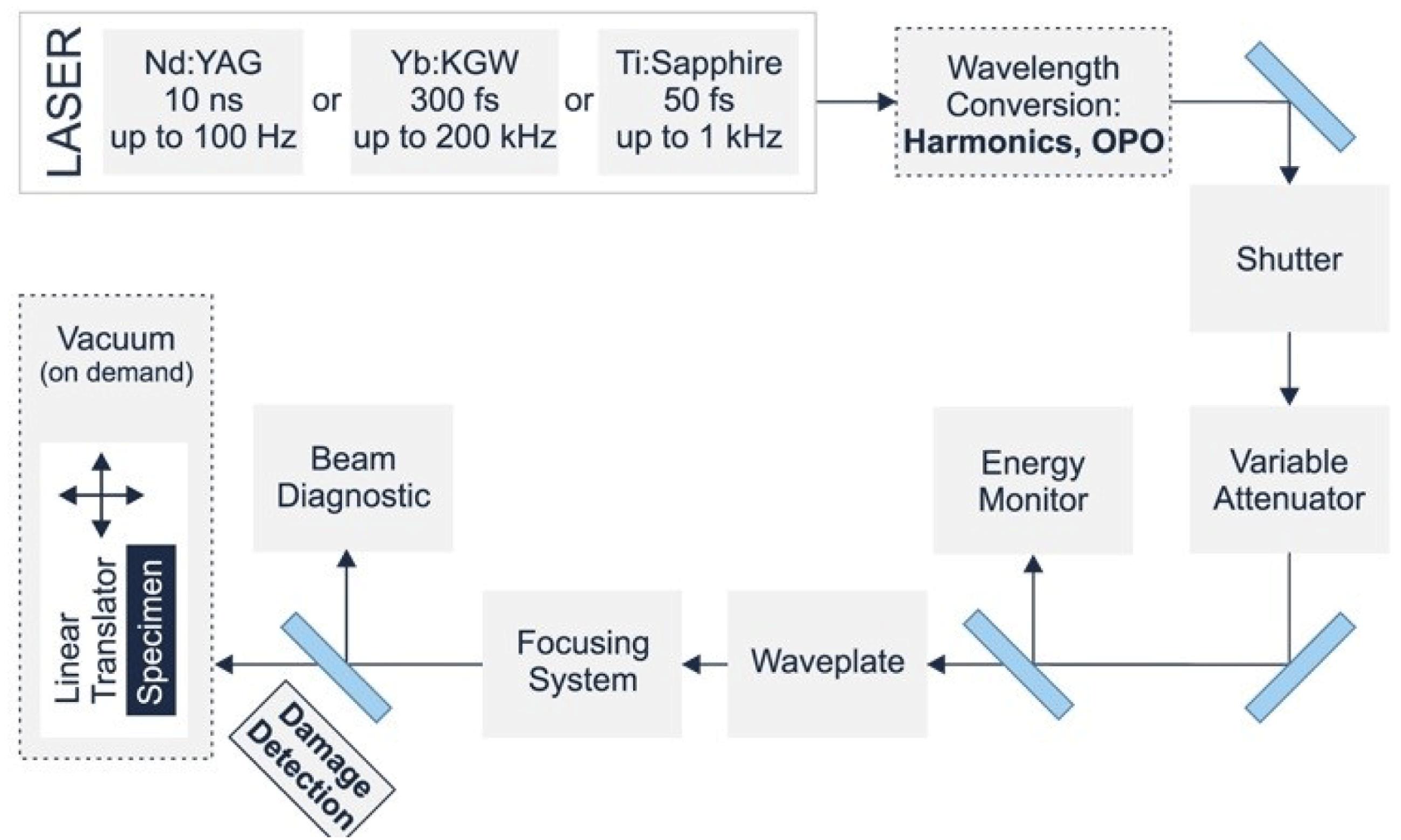
    Fig. 2. Block scheme of the LIDT testing setup at LIDARIS.
    Mirror surface; (a) map of exposure sites, red are noted as damaged according to the scattering light detection; (b) surface of damaged sample by Nomarski microscopy; (c) the sample surface superimposed with the map; (d) the corrected map of sites after the optical inspection.
    Fig. 3. Mirror surface; (a) map of exposure sites, red are noted as damaged according to the scattering light detection; (b) surface of damaged sample by Nomarski microscopy; (c) the sample surface superimposed with the map; (d) the corrected map of sites after the optical inspection.
    Damage threshold curves for AR-coated windows tested with ns pulses.
    Fig. 4. Damage threshold curves for AR-coated windows tested with ns pulses.
    Microscope images of sample 15 sites 69 and 200, marked as damaged, with notable scratches and dents not caused by laser.
    Fig. 5. Microscope images of sample 15 sites 69 and 200, marked as damaged, with notable scratches and dents not caused by laser.
    Damage threshold curves for HR dielectric mirrors tested with ns pulses.
    Fig. 6. Damage threshold curves for HR dielectric mirrors tested with ns pulses.
    Damage threshold curves for mirrors tested with ps pulses.
    Fig. 7. Damage threshold curves for mirrors tested with ps pulses.
    Damaged coating of the sample 10 (AR-coated window), where the sample was exposed to ns pulse trains; (a) the marked area of interest, (b) (from upper left) the site 47 (2 pulses at energy $170~\text{J}~\text{cm}^{-2}$); the site 48 (4 pulses at energy $170~\text{J}~\text{cm}^{-2}$); the site 42 (96 pulses at energy $170~\text{J}~\text{cm}^{-2}$); (c) a close look at the site 42; (d) 3D height topology (wire surface) of the site 42.
    Fig. 8. Damaged coating of the sample 10 (AR-coated window), where the sample was exposed to ns pulse trains; (a) the marked area of interest, (b) (from upper left) the site 47 (2 pulses at energy $170~\text{J}~\text{cm}^{-2}$); the site 48 (4 pulses at energy $170~\text{J}~\text{cm}^{-2}$); the site 42 (96 pulses at energy $170~\text{J}~\text{cm}^{-2}$); (c) a close look at the site 42; (d) 3D height topology (wire surface) of the site 42.
    Damaged coating of the sample 03 (the hybrid mirror), the sample was exposed to the train of ps pulses; (a) the marked area of interest, (b) the site 276 (407 pulses at the energy $1.47~\text{J}~\text{cm}^{-2}$); (c) the close look to the site 276; (d) 3D height topology (wire surface) of the site 276.
    Fig. 9. Damaged coating of the sample 03 (the hybrid mirror), the sample was exposed to the train of ps pulses; (a) the marked area of interest, (b) the site 276 (407 pulses at the energy $1.47~\text{J}~\text{cm}^{-2}$); (c) the close look to the site 276; (d) 3D height topology (wire surface) of the site 276.
    PulseMaximalPolarizationRepetition Spot beamEnvironment
    length pulses state rate diameter
    per site($1/e^{2}$, $0^{\circ }$ AOI)
    10 ns$10^{3}$P10 Hz0.245 mmAmbient air
    Table 1. Conditions for testing with nanosecond pulses.
    Sample no. Type Size/shapeAOI (deg.)
    09 HR mirror$1^{\prime \prime }$/round45
    10AR window$1^{\prime \prime }$/round0
    13AR window$1^{\prime \prime }$/round0
    14AR window$1^{\prime \prime }$/round0
    15AR window$1^{\prime \prime }$/round0
    16AR window$1^{\prime \prime }$/round0
    18AR window25 mm/round 0
    22 HR mirror40 mm/square 0
    Table 2. List of components tested at ns regime.
    Pulse PulsesPolarizationRepetitionSpot beamEnvironment
    lengthper site state rate diameter ($0^{\circ }$)
    1 ps$10^{5}$P1 kHz0.042 mmAmbient air
    Table 3. Conditions for testing with picosecond pulses.
    Sample no. TypeSize/shapeAOI (deg.)
    01 Hybrid mirror$1^{\prime \prime }$/round45
    02 Hybrid mirror$1^{\prime \prime }$/round45
    03 Hybrid mirror$1^{\prime \prime }$/round45
    05Protected silver mirror$1^{\prime \prime }$/round45
    07 Protected gold mirror$1^{\prime \prime }$/round45
    Table 4. List of components tested at ps regime.
    Sample Damage threshold ($\text{J}~\text{cm}^{-2}$)
    1073
    1317
    1438
    1528
    1645
    1823
    Table 5. Damage thresholds of AR-coated windows; linearly extrapolated values were rounded down to closest integer.
    Sample Damage threshold ($\text{J}~\text{cm}^{-2}$)
    0910
    2293
    Table 6. Damage thresholds of HR dielectric mirrors, linearly extrapolated values were rounded down to the closest integer.
    Sample Damage threshold ($\text{J}~\text{cm}^{-2}$)
    020.55
    031.25
    050.47
    070.51
    Table 7. Damage thresholds of mirrors, linearly extrapolated values were rounded down to two decimals.
    Jan Vanda, Jan ˇSevˇcík, Egidijus Pupka, Mindaugas ˇS ˇciuka, Andrius Melninkaitis, Martin Divok′y, Venkatesan Jambunathan, Stefano Bonora, V′aclav ˇSkoda, Antonio Lucianetti, Danijela Rostohar, Tomas Mocek, Valdas Sirutkaitis. Comparative LIDT measurements of optical components for high-energy HiLASE lasers[J]. High Power Laser Science and Engineering, 2016, 4(1): 01000e11
    Download Citation