• Photonics Research
  • Vol. 12, Issue 1, 1 (2024)
Yang Shi1、†, Xiang Li2、†, Mingjie Zou1, Yu Yu1、3、5、*, and Xinliang Zhang1、3、4、6、*
Author Affiliations
  • 1Wuhan National Laboratory for Optoelectronics & School of Optical and Electronic Information, Huazhong University of Science and Technology, Wuhan 430074, China
  • 2School of Mechanical Engineering and Electronic Information, China University of Geosciences, Wuhan 430074, China
  • 3Optics Valley Laboratory, Wuhan 430074, China
  • 4Xidian University, Xi’an 710126, China
  • 5e-mail: yuyu@mail.hust.edu.cn
  • 6e-mail: xlzhang@mail.hust.edu.cn
  • show less
    DOI: 10.1364/PRJ.495958 Cite this Article Set citation alerts
    Yang Shi, Xiang Li, Mingjie Zou, Yu Yu, Xinliang Zhang, "103 GHz germanium-on-silicon photodiode enabled by an optimized U-shaped electrode," Photonics Res. 12, 1 (2024) Copy Citation Text show less
    (a) Structural schematic of the waveguide Ge PD with a U-shaped electrode. The cross section of the silicon waveguide is 500 nm×220 nm and the silicon taper is 40 μm in length. Al, aluminum; Si, silicon; SiO2, silica. The equivalent circuit is shown including the transit time and RC parasitic parameters. The transit time is represented by the equivalent resistance Rt and the equivalent capacitance Ct. The RC parasitic parameters contain the junction capacitance Cj, series resistance RS, inductance Lp, and stray capacitance Cp as well as external load RL. (b) The top view of the conventional waveguide Ge PD with the parallel electrode. The dashed region represents RS. (c) The top view of the proposed PD with the U-shaped electrode. (d) The simulated RS versus LGe under two kinds of contact and corresponding reduction ratio of the series resistance. Reduction ratio=(RS,Parallel−RS,U-shaped)/RS,Parallel×100%. (e) The simulated bandwidth related to RS and on-electrode inductance Lp when Cj=16 fF.
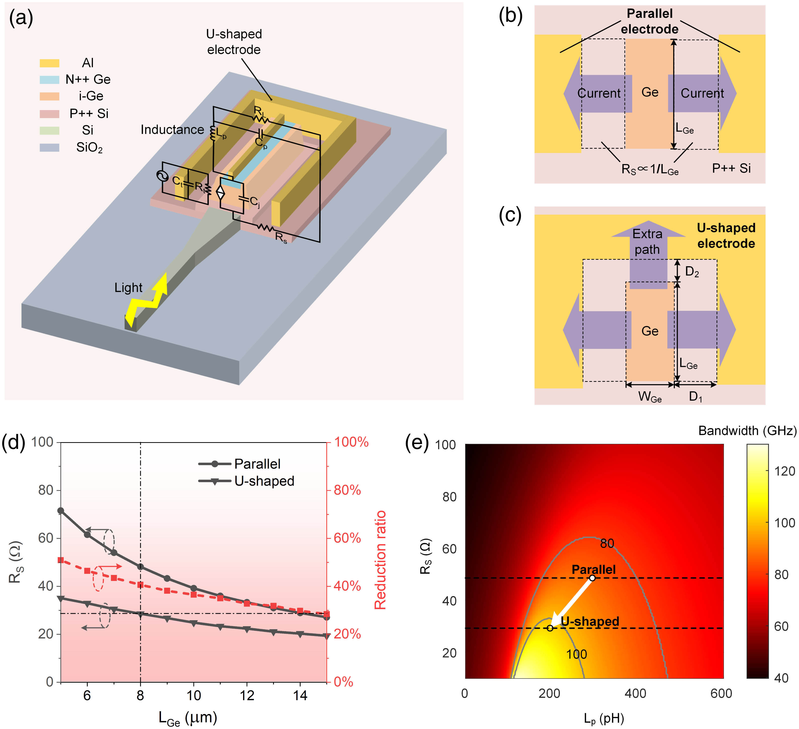
    Fig. 1. (a) Structural schematic of the waveguide Ge PD with a U-shaped electrode. The cross section of the silicon waveguide is 500  nm×220  nm and the silicon taper is 40 μm in length. Al, aluminum; Si, silicon; SiO2, silica. The equivalent circuit is shown including the transit time and RC parasitic parameters. The transit time is represented by the equivalent resistance Rt and the equivalent capacitance Ct. The RC parasitic parameters contain the junction capacitance Cj, series resistance RS, inductance Lp, and stray capacitance Cp as well as external load RL. (b) The top view of the conventional waveguide Ge PD with the parallel electrode. The dashed region represents RS. (c) The top view of the proposed PD with the U-shaped electrode. (d) The simulated RS versus LGe under two kinds of contact and corresponding reduction ratio of the series resistance. Reductionratio=(RS,ParallelRS,U-shaped)/RS,Parallel×100%. (e) The simulated bandwidth related to RS and on-electrode inductance Lp when Cj=16  fF.
    (a) The cross-section diagram of the PDs along the length direction. Si, silicon. (b) The microscope images of the fabricated PD with the U-shaped electrode. (c) The enlarged view of the active region and U-shaped electrode. (d) The measures I-V characteristics of the two kinds of PDs. (e) The measured photocurrent with the input optical power at −1 V. (f) The measured normalized S21 parameters of the PDs with U-shaped and parallel electrodes.
    Fig. 2. (a) The cross-section diagram of the PDs along the length direction. Si, silicon. (b) The microscope images of the fabricated PD with the U-shaped electrode. (c) The enlarged view of the active region and U-shaped electrode. (d) The measures I-V characteristics of the two kinds of PDs. (e) The measured photocurrent with the input optical power at 1  V. (f) The measured normalized S21 parameters of the PDs with U-shaped and parallel electrodes.
    Measured eye diagrams for 100/112/120 Gb/s OOK signals and 100/112/200 Gb/s PAM4 signals at −1 V.
    Fig. 3. Measured eye diagrams for 100/112/120 Gb/s OOK signals and 100/112/200 Gb/s PAM4 signals at −1 V.
    DeviceCj (fF)RS (Ω)Lp (pH)Cp (fF)RL (Ω)
    U-shaped22.612.9175.310.050
    Parallel24.020.1217.310.350
    Table 1. Extracted Parameters of the Electrical Elements
    Ref.TypeVoltage (V)R (A/W)ID (nA)BW (GHz)RBP (A·W1·GHz)D* (cm·Hz1/2·W1)
    [23]InP/InGaAs−20.20.1270141.61×109
    [24]MoTe2−30.210–1000244.81.22×109
    [25]Graphene−0.30.4>40161.5×109
    [26]Ge, lateral−11.010070701.77×109
    [27]Ge, lateral−10.742.567506.78×109
    [14]Ge, lateral−20.3<20026579.52.37×108
    0.45<1002401085.03×108
    [19]Ge, vertical−30.896.48071.21.33×1010
    [21]Ge, vertical−21.056.467701.44×1010
    [18]Ge, vertical−30.813575614.84×109
    This workGe, vertical−10.951.3103982.95×1010
    Table 2. Literature Overview of the State-of-the-Art High-Speed Waveguide PDs Integrated on Silicona
    Yang Shi, Xiang Li, Mingjie Zou, Yu Yu, Xinliang Zhang, "103 GHz germanium-on-silicon photodiode enabled by an optimized U-shaped electrode," Photonics Res. 12, 1 (2024)
    Download Citation