1Wuhan National Laboratory for Optoelectronics & School of Optical and Electronic Information, Huazhong University of Science and Technology, Wuhan 430074, China
2School of Mechanical Engineering and Electronic Information, China University of Geosciences, Wuhan 430074, China
【AIGC One Sentence Reading】:An optimized U-shaped electrode boosts germanium photodiode performance, achieving a record 103 GHz bandwidth and high detectivity, vital for fast chip-based photodetection in data communication.
【AIGC Short Abstract】:A novel U-shaped electrode design has been introduced to enhance the performance of germanium photodiodes in silicon photonic circuits. This innovation significantly reduces the parasitic resistance-capacitance effect, boosting bandwidth to a record-high 103 GHz without compromising other key performance metrics. The photodiode exhibits excellent responsivity and low dark current, enabling ultra-fast photodetection for high-capacity data communication.
Note: This section is automatically generated by AI . The website and platform operators shall not be liable for any commercial or legal consequences arising from your use of AI generated content on this website. Please be aware of this.
Abstract
High-performance germanium photodiodes are crucial components in silicon photonic integrated circuits for large-capacity data communication. However, the bandwidths of most germanium photodiodes are limited by the intractable resistance–capacitance parasitic effect. Here, we introduce a unique U-shaped electrode to alleviate this issue, reducing the parasitic effect by 36% without compromising any other performance. Experimentally, a large bandwidth of 103 GHz, an optical responsivity of 0.95 A/W at 1550 nm, and a dark current as low as 1.3 nA are achieved, leading to a record high specific detectivity. This is the first breakthrough to 100 GHz bandwidth among all vertical germanium photodiodes, to the best of our knowledge. Open eye diagrams of 120 Gb/s on-off keying and 200 Gb/s four-level pulse amplitude signals are well received. This work provides a promising solution for chip-based ultra-fast photodetection.
1. INTRODUCTION
In the past decade, silicon photonics has made great advances and is widely used in optical communication [1], high-performance computing [2], and quantum signal processing [3]. Due to the complementary metal-oxide-semiconductor (CMOS)-compatible fabrication and feasibility of monolithic integration with microelectronic devices, silicon photonic integrated circuit (SiPIC) is promising to significantly reduce cost and power consumption while increasing integration density [4,5]. Waveguide-integrated germanium (Ge) photodiodes (PDs), being responsible for converting optical signals into electrical form, are key elements in the SiPICs. With the explosive growth of global communication capacity, waveguide PDs with bandwidth surpassing 100 GHz have become a subject of intense research for several decades [6,7]. Among all materials, mainly indium phosphide (InP) or graphene-based PDs enable this goal, owing to the very high carrier mobility [8–11]. Several Ge PDs with bandwidth have been reported thanks to the very narrow intrinsic Ge regions and the reduced carrier transit time [12,13]. Recently, devices with narrow Ge fin sandwiched between in situ-doped silicon layers were reported with a bandwidth of 265 GHz [14]. However, the optical responsivities and dark current were compromised due to the narrow intrinsic regions.
Typically, the ultimate bandwidth of a Ge PD is determined by the carrier transit time, and an intrinsic region of 300–400 nm corresponds to a bandwidth of 100 GHz [15]. Although such an intrinsic region is routinely utilized, the practical bandwidth is much below the desired value, primarily limited by the resistance–capacitance parasitic effect. To address this issue, the gain-peaking technology has been proposed to partly offset parasitic capacitance [16–18]. Previous work has further demonstrated that reducing series resistance and matching it with a proper on-electrode inductance can boost the bandwidth, enabling an 80 GHz bandwidth [19]. Nevertheless, in conventional waveguide Ge PDs, shrinking series resistance is limited by the design trade-off with junction capacitance. Typically, the metal electrodes in these devices are parallel to the Ge film (denoted as parallel electrode). As a result, Ge length affects the carrier collection path and thus the cross-section area of the series resistance. This means that reducing series resistance by increasing Ge length in turn increases the junction capacitance, keeping the resistance–capacitance product unchanged.
Here, we demonstrate a high-speed waveguide Ge PD using a specifically designed U-shaped electrode. By establishing an extra carrier collection path to extend the resistance area, the series resistance is lowered by 36% without increasing junction capacitance. On this base, an optimal on-chip inductance is further introduced to partly offset parasitic capacitance. Experimentally, the bandwidth is improved from 83 to 103 GHz, compared with the parallel electrode (also with an optimal inductance). To the best of our knowledge, this is the first vertical Ge PD with a bandwidth greater than 100 GHz. Under the voltage of , the measured optical responsivity at 1550 nm is 0.95 A/W and the dark current is as low as 1.3 nA, resulting in a record high specific detectivity of . Open eye diagrams of 120 Gb/s on-off keying (OOK) and 200 Gb/s four-level pulse amplitude (PAM4) signals are obtained for high-speed demonstration. This work provides design guidance for high-speed optoelectronic devices and paves the way for ultra-fast optical interconnects.
Sign up for Photonics Research TOC. Get the latest issue of Photonics Research delivered right to you!Sign up now
2. OPERATION PRINCIPLE AND DEVICE DESIGN
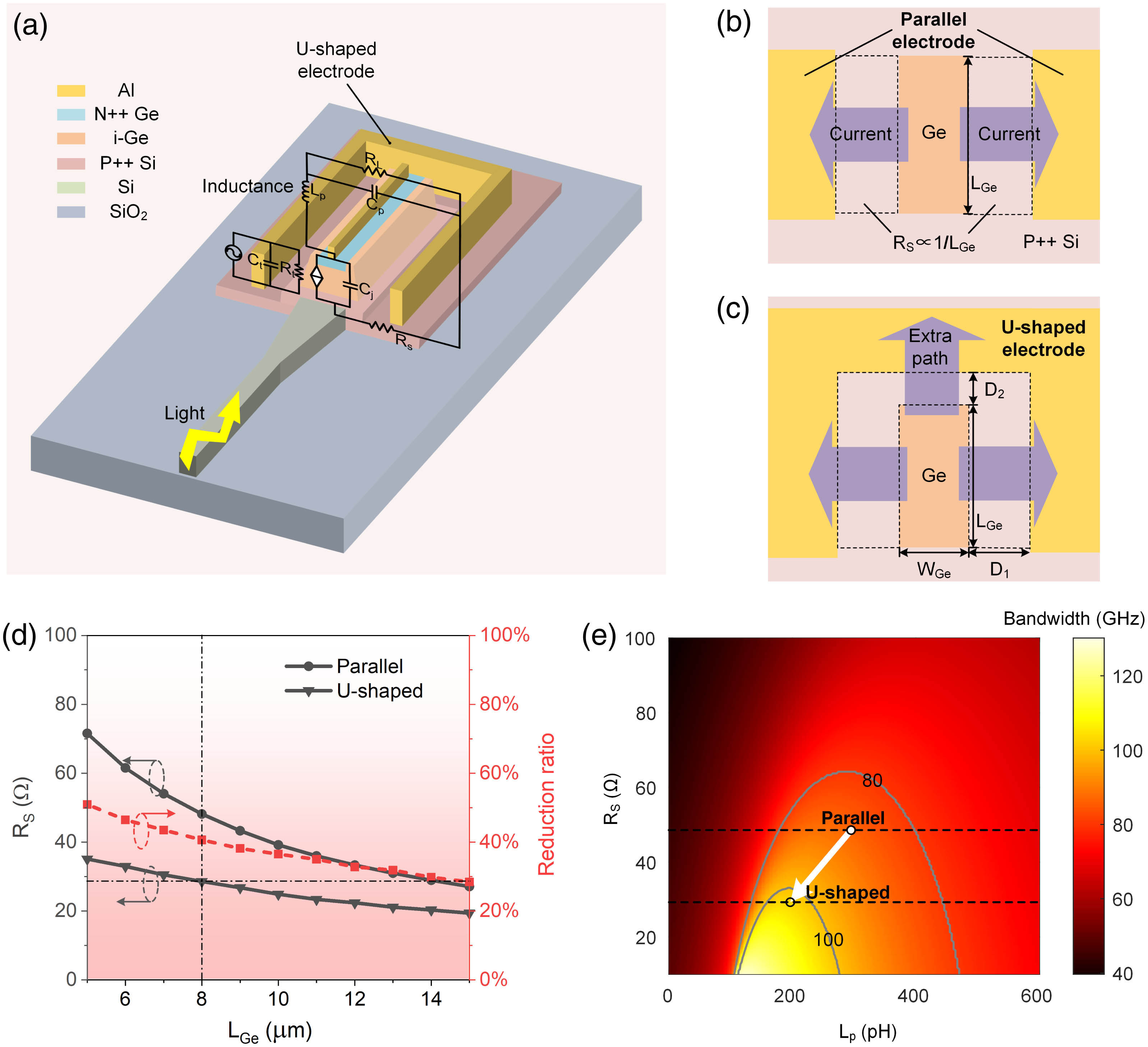
The structural schematic of the proposed waveguide Ge PD with the U-shaped electrode and the equivalent circuit are shown in Fig. 1(a). The active region is a vertical n-i-p junction consisting of 50 nm Ge, 350 nm intrinsic Ge (i-Ge), and silicon. The 350 nm intrinsic region corresponds to a carrier transit time-determined bandwidth of 120 GHz. Being different from conventional waveguide PDs, the specifically designed U-shaped electrode increases the resistance area and reduces the series resistance without increasing the capacitance. The capacitance is further mitigated by an optimal on-electrode inductance, provided by the metal connection between the PD and pad.
Figure 1.(a) Structural schematic of the waveguide Ge PD with a U-shaped electrode. The cross section of the silicon waveguide is and the silicon taper is 40 μm in length. Al, aluminum; Si, silicon; SiO2, silica. The equivalent circuit is shown including the transit time and RC parasitic parameters. The transit time is represented by the equivalent resistance and the equivalent capacitance . The RC parasitic parameters contain the junction capacitance , series resistance , inductance , and stray capacitance as well as external load . (b) The top view of the conventional waveguide Ge PD with the parallel electrode. The dashed region represents . (c) The top view of the proposed PD with the U-shaped electrode. (d) The simulated versus under two kinds of contact and corresponding reduction ratio of the series resistance. . (e) The simulated bandwidth related to and on-electrode inductance when .
The junction parasitic parameter consists of the series resistance and junction capacitance . Unfortunately, there is a design trade-off between them under parallel electrode [Fig. 1(b)]. Specifically, is from an analogous plate capacitor proportional to the Ge area, i.e., Ge length when the width is fixed. is a resistance perceived by the photocurrent flowing from the Ge region to the electrode, and thus it is inversely proportional to the collection cross section of the silicon layer, i.e., Ge length when silicon thickness is fixed. As a result, the product of and is independent of the Ge length, and it is difficult to reduce and concurrently by solely tailoring the Ge geometry. We introduce a U-shaped electrode to alleviate this issue, as shown in Fig. 1(c). By connecting the metal electrodes on both sides of Ge, an extra carrier collection path is established, increasing the series resistance area (i.e., reducing ). Thanks to the unchanged Ge length, the junction capacitance is not increased. It should be noted that the perceived resistance along each of the three carrier collection paths must be equal. Otherwise, the photocurrent tends to concentrate on the path with the lowest resistance, resulting in the discount of previously indicated series resistance reduction strategy. To make it, the space between the Ge edge and the U-shaped electrode should match a design criterion, for a rectangular Ge region typically with unequal length and width: where and are the width and length of the Ge region, while and represent the gaps from the Ge length edge and width edge to the electrode, respectively. Under this condition, the simulated versus adopting two kinds of electrode is shown in Fig. 1(d). In both cases, decreases inversely with Ge length, and it is reduced by 30%–50% under the U-shaped electrode compared with the parallel one. The and are selected to be 8 and 5 μm to ensure sufficient optical absorption at 1550 nm and a low junction capacitance (). Here, the Ge width of 5 μm is chosen by comprehensively considering the optical absorption and fabrication capability. If the fabrication process permits, an appropriate reduction of the Ge width can be expected to further reduce the junction capacitance . Under this circumstance, is reduced from 48 to 28 Ω with a ratio of 40.6%. If the parallel electrode is adopted, the Ge length needs to extend from 8 to 14 μm to achieve the same decrease, while the junction capacitance is increased by 75%. Finally, needs to be 0.625, and μ and μ are selected.
We show that reducing the series resistance is important to the bandwidth. Figure 1(e) presents the simulated bandwidth related to and on-electrode inductance under , using the equivalent circuit shown in Fig. 1(a). The gray solid lines denote the bandwidths of 80 and 100 GHz, and the black dashed lines represent the series resistances under parallel and U-shaped electrodes, respectively. It can be observed that when is constant, the bandwidth increases as the decreases. While remains constant, the bandwidth first increases and subsequently decreases with . Therefore, there is an optimal to maximize the bandwidth. The bandwidth under the U-shaped electrode (with ) is increased from 87 to 110 GHz compared with the parallel electrode (with ). The 110 GHz bandwidth approaches the theoretical limit of the 350 nm intrinsic region.
3. EXPERIMENTAL RESULTS
To investigate the influence of using the U-shaped electrode, we fabricated two PDs with U-shaped and conventional parallel electrodes, respectively. The one with the U-shaped electrode is matched with a 220 pH inductance and the other with the parallel electrode adopts a 300 pH inductance. Figure 2(a) shows the cross-section diagram of the PDs along the length direction. The PDs are fabricated using a silicon-on-insulator wafer with a 220 nm thick silicon top layer and a 2 μm buried oxide layer. The silicon layer is etched into the ridge waveguide with a 90 nm slab. Then, the silicon top layer is doped using boron of . A 400 nm Ge is deposited on the doping region of the silicon, and doping of phosphorus is implanted on the top of the Ge to form the vertical n-i-p junction. The metals contacted to Ge and silicon are fabricated, and subsequently a second metal layer is fabricated to form different inductances. The two PDs are identical except for the silicon-contacted electrode and matching inductance. The microscope image of the fabricated PD with the U-shaped electrode is shown in Fig. 2(b). Here, a middle electrode with length of 195 μm and thickness of 2 μm is adopted for the desired 220 pH inductance. For the parallel one, the length is set as 245 μm for a 300 pH inductance. The detail of the red dashed region is shown in Fig. 2(c), and the Ge region and the U-shaped electrode are highlighted.
Figure 2.(a) The cross-section diagram of the PDs along the length direction. Si, silicon. (b) The microscope images of the fabricated PD with the U-shaped electrode. (c) The enlarged view of the active region and U-shaped electrode. (d) The measures I-V characteristics of the two kinds of PDs. (e) The measured photocurrent with the input optical power at . (f) The measured normalized parameters of the PDs with U-shaped and parallel electrodes.
The current-voltage (I-V) characteristics of the two PDs are measured, as shown in Fig. 2(d). The photocurrent is measured at 1550 nm under a received optical power of , by extracting the coupling loss of 4.6 dB (denoted as ) according to a referenced grating coupler. The photocurrents and dark currents of the two PDs are similar under different bias voltages, indicating that the U-shaped electrode does not degrade the static performance. Very low dark currents of 1.3 and 1.9 nA are measured at for the U-shaped and parallel electrodes, respectively. Even at , the dark currents are lower than 7 nA. The good dark current performance is contributed by the robust fabrication process and compact Ge footprint. The photocurrent is almost constant under 0 to owing to the built-in electric field that is capable of sweeping out most of the photo-generated carriers within their lifetime. Then, we measure the photocurrent () under different optical power input to the grating coupler (). The relation is plotted and linearly fitted, where represents the optical power fed into the PD by extracting the coupling loss. The slope of the fitted straight line is the measured optical responsivity. The measured photocurrents with different input optical power at are shown in Fig. 2(e), and the optical responsivities are 0.95 and 0.92 A/W for the U-shaped and parallel PDs, respectively. The former shows a slightly higher responsivity possibly due to higher carrier collection efficiency under a longer collection length [20].
Small-signal radio-frequency measurements are carried out using a 110 GHz light component analyzer (Keysight N4372E) in the test range of 10 MHz to 110 GHz. The Impedance Standard Substrate is used to calibrate the bias-tee, cables, and microprobe. The measured normalized parameters are shown in Fig. 2(f). For the PD with the U-shaped electrode, the bandwidths are 13, 59, and 103 GHz under voltages of 0, , and , respectively. The relatively lower bandwidths at 0 and result from the slower carrier movement than the saturation velocity. The bandwidth reaches its maximum at and exceeds 100 GHz. Similarly, the maximum bandwidth of 83 GHz under the parallel situation is also obtained at , as shown in Fig. 2(f) for reference. We fit the measured parameters using the equivalent circuit model from 10 MHz to 110 GHz and Table 1 shows the extracted parameters. The series resistance of the PD with the U-shaped electrode is 12.9 Ω, while the value is 20.1 Ω for the PD with the conventional parallel electrode. This indicates 36% reduced series resistance. The RC-limited bandwidth is also simulated to be 155 GHz, and thus the total bandwidth of 103 GHz is limited by the carrier transit time. These results indicate that the U-shaped electrode enables reducing series resistance and improving bandwidth.
Extracted Parameters of the Electrical Elements
Device
(fF)
(Ω)
(pH)
(fF)
(Ω)
U-shaped
22.6
12.9
175.3
10.0
50
Parallel
24.0
20.1
217.3
10.3
50
The high-speed performance of the U-shaped PD is characterized via eye diagrams using a real-time digital storage oscilloscope with 256 GSa/s sampling rate (Keysight UXR0594AP). An OOK or PAM4 signal with a pattern length of is generated by an arbitrary waveform generator (Keysight M8199A) and amplified by a 45 GHz high-speed driver. A 40 GHz Mach–Zehnder modulator is adopted to modulate the continuous-wave light. The optical signal is fed into the fabricated PD and the resulting electrical signal is collected by the oscilloscope. The post-compensation and offline digital signal process is carried out to deduct the distortion of high-speed electrical signals through the cables and the transmitter [21,22]. As shown in Fig. 3, we measure the eye diagrams for 100, 112, and 120 Gb/s OOK signals by setting the input optical power as , , and . The signal-to-noise ratios (SNRs) are 14.76, 12.13, and 11.12 dB, respectively. Furthermore, the PD is used to receive 100, 112, and 200 Gb/s PAM4 signals, under the input optical power of , , and . The SNRs are 25.39, 23.89, and 19.44 dB, respectively. These results make the proposed PD very competitive to satisfy the demands in the application with large-capacity data transmissions.
Figure 3.Measured eye diagrams for 100/112/120 Gb/s OOK signals and 100/112/200 Gb/s PAM4 signals at −1 V.
Table 2 presents the literature overview of the state-of-the-art high-speed silicon-based PDs. InP and two-dimensional material PDs achieve bandwidths of several tens of gigahertz, while the optical responsivities are typically low due to the weak optical coupling and light–matter interaction [23–25]. They also suffer from relatively complex fabrication. The waveguide Ge PDs benefit from CMOS-compatible fabrication, and they can be divided into vertical and lateral types according to the spatial distribution direction of the p-i-n junction. The lateral Ge PDs are practically easier to achieve narrow intrinsic regions and thus larger bandwidths. For instance, Ref. [14] achieves an ultra-high bandwidth up to 265 GHz through a 100 nm intrinsic region. However, the responsivity and dark current inevitably deteriorate. Furthermore, a more complex process is required, including chemical mechanical polishing and Ge corrosion. The vertical Ge PDs are more popular due to the simple fabrication process and robust manufacturing. However, the bandwidth improvement has become even more difficult due to relatively larger volume, and previous works exhibit responsivities of 0.8–1 A/W and bandwidths of 67–80 GHz. This work is the first vertical Ge PD with a bandwidth greater than 100 GHz. We attribute this result to the optimized parasitic parameters comprehensively regulated by the U-shaped electrode and on-electrode inductance. Meanwhile, thanks to the high responsivity, the responsivity-bandwidth product of is also the highest result among the vertical PDs.
Literature Overview of the State-of-the-Art High-Speed Waveguide PDs Integrated on Silicona
Ref.
Type
Voltage (V)
(A/W)
(nA)
BW (GHz)
RBP ()
()
[23]
InP/InGaAs
−2
0.2
0.12
70
14
[24]
−3
0.2
10–1000
24
4.8
[25]
Graphene
−0.3
0.4
–
[26]
Ge, lateral
−1
1.0
100
70
70
[27]
Ge, lateral
−1
0.74
2.5
67
50
[14]
Ge, lateral
−2
0.3
265
79.5
0.45
240
108
[19]
Ge, vertical
−3
0.89
6.4
80
71.2
[21]
Ge, vertical
−2
1.05
6.4
67
70
[18]
Ge, vertical
−3
0.81
35
75
61
This work
Ge, vertical
−1
0.95
1.3
103
98
, responsivity; , dark current; BW, bandwidth; RBP, responsivity-bandwidth product; , specific detectivity.
For data communication, responsivity and dark current comprehensively determine the sensitivity of the optical receiver, which is crucial for reducing power consumption, relaxing the requirement of high-power lasers, and suppressing optical nonlinearity. The specific detectivity () is used to evaluate the sensitivity, taking into account both responsivity and dark current [28,29]. This work has reached the highest specific detectivity of among these Ge PDs due to ultra-low dark current. Although Ref. [21] has a higher responsivity, it has higher dark current, therefore having a slightly lower . Overall, this work provides a simple-fabrication, high-speed, and highly sensitive PD for the SiPICs and optical interconnects.
In addition to the Ge PIN PD, the SiGe avalanche photodiode (APD) is also important for optical interconnects, and it typically provides 5–10 dB higher sensitivity due to the internal gain by applying a high voltage to provide a strong electric field in the intrinsic Si region for impact ionization [30]. Several investigations suggested a thin intrinsic Si [31] or PIN structure with Ge multiplication [32] to reduce the bias voltage. On the other hand, the bandwidths of SiGe APDs are typically lower than that of the PIN PDs, and schemes with thin intrinsic region [31] and resonance effect [33] were demonstrated to improve the bandwidth.
5. CONCLUSION
In conclusion, we demonstrate that the optimal U-shaped electrode can improve PD bandwidth compared with the conventional PD. At , the measured 3 dB bandwidth is 103 GHz, together with high responsivity and ultra-low dark current. High-speed optical reception based on the proposed PD is demonstrated with 120 Gb/s OOK and 200 Gb/s PAM4 signals. This work may pave the way for chip-based optical receivers in ultra-high-speed optical interconnects.
[11] S. M. Koepfli, M. Eppenberger, M. S.-B. Hossain. >500 GHz bandwidth graphene photodetector enabling highest-capacity plasmonic-to-plasmonic links. European Conference on Optical Communication (ECOC), 1-4(2022).
[13] S. Lischke, A. Peczek, F. Korndörfer. Ge photodiode with −3 dB OE bandwidth of 110 GHz for PIC and ePIC platforms. IEEE International Electron Devices Meeting (IEDM), 7.3.1-7.3.4(2020).
 AI Video Guide
  AI Picture Guide
 AI One Sentence