Chaoqun Niu, Yaqing Pang, Zhi Liu, Buwen Cheng. Research progress of mid-infrared silicon-based modulators (Invited)[J]. Infrared and Laser Engineering, 2022, 51(3): 20220021
Search by keywords or author
- Infrared and Laser Engineering
- Vol. 51, Issue 3, 20220021 (2022)
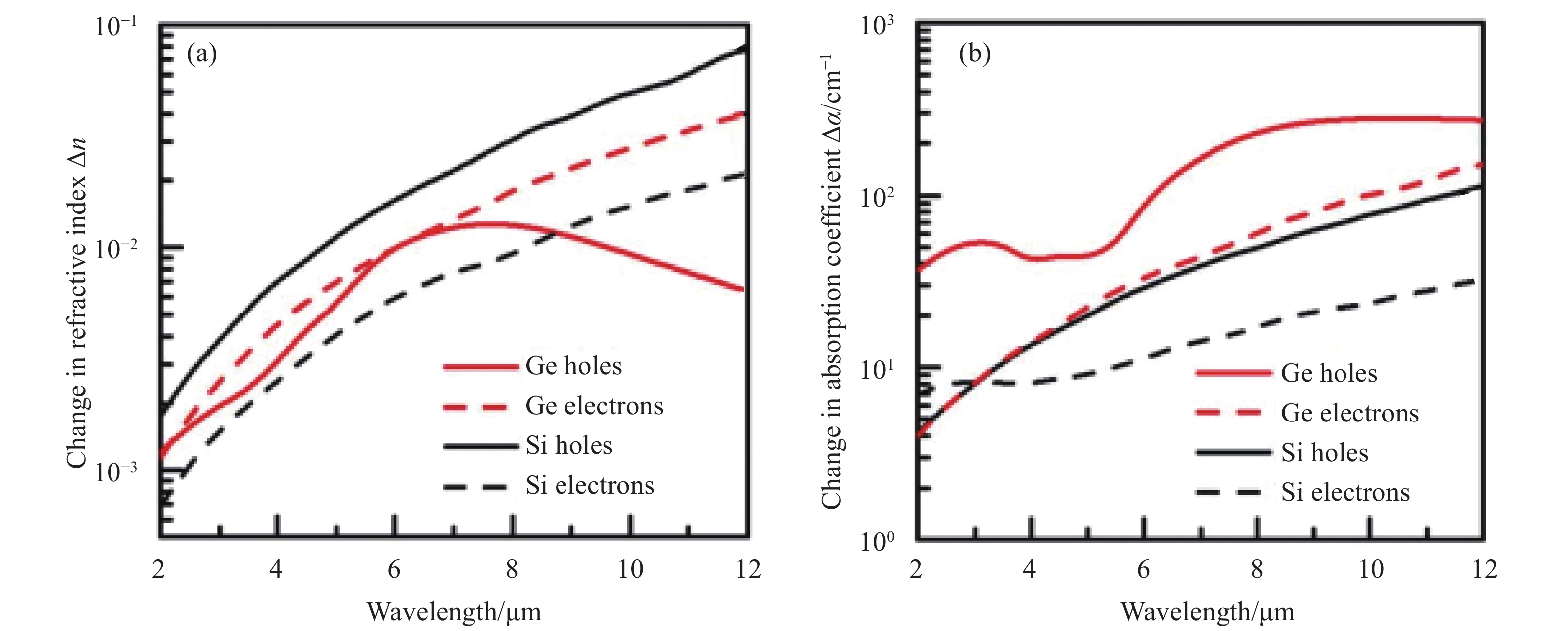
![Comparisons of (a) change in refractive index and (b) change in absorption coefficient at in Si and Ge materials[20]](/richHtml/irla/2022/51/3/20220021/img_1.jpg)
Fig. 1. Comparisons of (a) change in refractive index and (b) change in absorption coefficient at in Si and Ge materials[20]
![(a) Optical microscope image of the fabricated MZI modulator. Inset: Magnified detail of the 50/50 Y-junction, differential optical path imbalance, thermo-optic heaters, and RF signal input end; (b) Simulated intensity profile of the fundamental quasi-TE mode at λ = 2165 nm; (c) Cross-section schematic of the PIN diode waveguide active region[21]](/richHtml/irla/2022/51/3/20220021/img_2.jpg)
Fig. 2. (a) Optical microscope image of the fabricated MZI modulator. Inset: Magnified detail of the 50/50 Y-junction, differential optical path imbalance, thermo-optic heaters, and RF signal input end; (b) Simulated intensity profile of the fundamental quasi-TE mode at λ = 2165 nm; (c) Cross-section schematic of the PIN diode waveguide active region[21]
Fig. 3. (a) Schematic cross section of the SOI PIN junction[22]; (b) Optical microscope image of the spiral-shaped PIN electroabsorption modulator. P++ doped areas have been artificially colored in red, and N++ doped areas have been colored in blue[22]; (c) Normalized transmission versus drive current at 1.31 µm, 1.55 µm, 2 µm and 2.5 µm[23]
Fig. 4. (a) Process flow of Ge-on-insulator wafer fabrication; (b) TEM cross-sectional image of the fabricated Ge-on-insulator wafer; (c) Scanning electron microscope image of a GeOI modulator and (d) attenuation characteristics of the Ge variable optical attenuator in the 2 μm band as a function[24]
Fig. 5. (a) Optical microscope image of the device; (b) Cross-section diagram of the PIN junction[25]. Captured LWIR camera image with the QCL tuned to λ =8 μm; (c) When the laser is emitting; (d) When the “laser off” frame is subtracted from the “laser on” frame. White areas show high infrared light intensity, and dark areas show low intensity[16]
Fig. 6. (a) Cross-section of the phase shifter for MZI modulator and microring modulator; Optical microscope image of (b) the microring modulator and (c) the MZI modulator[26]
Fig. 7. (a) MZI modulator based on SOI platform[28]; (b) Cross-sectional schematic diagram of the MZI modulator’s active arms and (c) optical microscope image of the traveling-wave MZI modulator in Ref.[29]
Fig. 8. Ge-on-Si platform: (a) SEM cross section and (b) top view of device of fully undercutting heater. Ge-on-SOI platform: (c) SEM cross section and (d) top view of device of fully undercutting heater[30]
Fig. 9. (a) Plan-view microscope image of the fabricated TO phase shifter in Ref. [31] ; (b) Micrographs of the fabricated TO phase shifter in Ref. [32]
|
Table 1. Types and performance of mid-infrared silicon-based electro-optic modulators

Set citation alerts for the article
Please enter your email address


