Author Affiliations
1Department of Chemistry, The University of Tokyo, Tokyo 113-0033, Japan2Department of Electrical Engineering and Information Systems, The University of Tokyo, Tokyo 113-0033, Japan3Department of Electronic Engineering, The Chinese University of Hong Kong, Shatin, Hong Kong SAR, China4Department of Electrical Engineering, University of California, Los Angeles, California 90095, USA5e-mail: goda@chem.s.u-tokyo.ac.jpshow less
Abstract
Mid-infrared (MIR) integrated photonics has attracted broad interest due to its promising applications in biochemical sensing, environmental monitoring, disease diagnosis, and optical communication. Among MIR integration platforms, germanium-based platforms hold many excellent properties, such as wide transparency windows, high refractive indices, and high nonlinear coefficients; however, the development of MIR germanium photonic devices is still in its infancy. Specifically, MIR high- germanium resonators with comparable performance to their silicon counterparts remain unprecedented. Here we experimentally demonstrate an MIR germanium nanocavity with a factor of , the highest-to-date of reported nanocavities across MIR germanium-based integration platforms. This is achieved through a combination of a feasible theoretical design, Smart-Cut methods for wafer development, and optimized device fabrication processes. Our nanocavity, with its high factor and ultrasmall mode volume, opens new avenues for on-chip applications in the MIR spectral range.1. INTRODUCTION
Mid-infrared (MIR) integrated photonics has attracted broad interest due to promising applications in biochemical sensing, environmental monitoring, disease diagnosis, and optical communication [1]. A variety of integration platforms for MIR applications have been reported to date. These have covered a diverse range of optical materials, including noble metals [2], two-dimensional materials [3], chalcogenide glasses [4], and Group IV semiconductors (silicon and germanium) [5–8]. Integration platforms based on Group IV semiconductors have the notable advantages of low optical loss and excellent CMOS process compatibility, which are critical for practical applications with low-cost and high-volume production requirements [9].
A large number of MIR photonic integrated devices have been demonstrated experimentally in silicon-based platforms; these include silicon-on-sapphire waveguides [10,11], silicon-on- waveguides [12], silicon-on- waveguides [13], silicon microring resonators [14], and silicon photonic crystal cavities [15,16]. Based on these platforms, various photonic devices with state-of-the-art performance have been demonstrated recently in the MIR spectral region. For example, a photonic crystal nanocavity with a quality () factor of has been demonstrated on a silicon platform by virtue of mature silicon fabrication techniques [16]. However, due to the limited transparency window of silicon, silicon photonic devices are not capable of working at wavelengths above 8 μm [17].
Germanium offers several key advantages over silicon: a wider spectral transparency window (2–15 μm), a higher refractive index (), and a higher third-order nonlinear susceptibility () [18]. A number of preliminary MIR germanium photonic devices have been demonstrated in recent years, including germanium-on-SOI (silicon-on-insulator) waveguides [19,20], germanium-on- waveguides [21], germanium-on-insulator (GOI) waveguides [22,23], suspended germanium devices [24,25], and silicon–germanium waveguides [26]. Despite these results, the development of MIR germanium photonic devices is still in its infancy due to lack of significant advance in the quality of germanium devices. Specifically, MIR high- germanium resonators with comparable or superior performance to their silicon counterparts remain unprecedented.
Sign up for Photonics Research TOC. Get the latest issue of Photonics Research delivered right to you!Sign up now
In this paper, we present an MIR germanium nanocavity with a factor of and an effective mode volume of . It is worthwhile mentioning that this factor is the highest of reported nanocavities across MIR germanium-based integration platforms. Such a high- nanocavity is achieved by a combination of an experimentally feasible theoretical design, Smart-Cut methods for GOI wafer development, and optimized device fabrication processes. By virtue of its high value and an ultrasmall mode volume, our nanocavity enables unprecedented strong light–matter interaction in the MIR spectral range, which is expected to enable promising applications in on-chip sensing, spectroscopy, nonlinear optics, optomechanics, and quantum information processing in the MIR spectral region.
2. THEORETICAL DESIGN OF THE MIR HIGH-Q GERMANIUM NANOCAVITY
Our MIR germanium nanocavity is a photonic crystal nanobeam cavity connected to two focusing subwavelength grating couplers by suspended-membrane waveguides. The schematic diagram of the device is shown in Fig. 1. All components are integrated monolithically on a GOI chip. The magnified central part of the device, that is, the photonic crystal nanobeam cavity, is shown in the inset to the left. The photonic crystal nanobeam consists of a 700-nm-wide waveguide and 18 air through-holes with varying diameters. The sizes and spacing of the air through-holes are symmetrical across the midpoint of the nanobeam, between the ninth and tenth holes. From either end, the first four through-holes have equal diameters, of 410 nm (). From the fifth to the ninth through-hole, the diameters are parabolically tapered from 370 nm () to 240 nm (). The distances between the first five through-holes are all 600 nm (), whereas the distances between the fifth to tenth through-holes are parabolically tapered from 550 nm () to 480 nm (). This parabolic tapering configuration is designed to reduce radiation loss induced by impedance mismatch, by providing a slowly varying effective-refractive-index environment for the resonant mode of the nanobeam cavity. A schematic of the cross-section of the suspended-membrane waveguide is illustrated in the inset to the right in Fig. 1. The waveguide, with an etching depth () of 150 nm, is fabricated in a top germanium layer () with a thickness of 300 nm. Buried oxide (BOX) and layers () with a combined thickness of 2 μm are designed to be removed by hydrofluoric acid (HF) to form an air-cladding structure. This structure provides a symmetric refractive index environment for excellent light confinement.
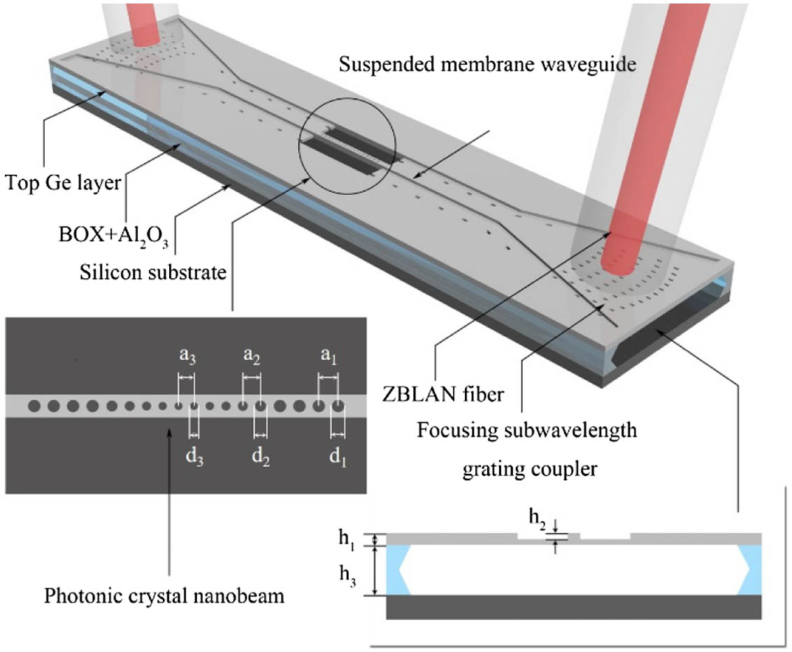
Figure 1.Schematic of the monolithically integrated on-chip MIR germanium device that contains a high- nanocavity, two suspended-membrane waveguides, and two focusing subwavelength grating couplers. The inset to the bottom left shows the design of the high- nanocavity. The inset to the bottom right shows a cross-sectional view of a suspended-membrane waveguide.
3. FABRICATION OF THE MIR HIGH-Q GERMANIUM NANOCAVITY
Based on the above design, we built an MIR high- germanium nanocavity. First, we fabricated a high-quality GOI wafer by using Smart-Cut methods [22]. We first deposited a capping layer on bulk monocrystalline germanium via plasma-enhanced chemical vapor deposition, and then removed it by wet etching after ion implantation. Next, we deposited 5-nm-thick layers as bonding interfaces on the surfaces of the germanium and a pre-prepared -covered silicon wafer by using atomic layer deposition. After bonding the wafer, we performed a wafer-splitting process by annealing, and then polished the split germanium surface by chemical-mechanical planarization. Lastly, annealing was performed again to improve the surface quality of the GOI wafer. After the GOI wafer fabrication, we fabricated our device on the wafer by using optimized processes in two cycles. In the first cycle, we used standard electron-beam lithography (EBL) to define the layouts of the nanocavity, grating couplers, and air holes along the suspended-membrane ridge waveguides, on a 400-nm-thick ZEP 520A resist layer pre-spin-coated on the GOI chip. Then these layouts were fully etched and transferred to the top germanium layer using a commercial inductively coupled plasma (ICP) etcher, with a mix of and gases. In the second cycle, the suspended-membrane waveguide was defined by EBL and half-etched with the ICP etcher, using gas. Finally, we eliminated the part of the BOX layer under the device by soaking the chip in a dilute solution of HF. The acid permeated through the pre-defined air holes and etched out the part of the BOX layer under the device to form the air-cladding structure. A scanning electron microscope (SEM) image of the fabricated device is shown in Fig. 2(a), whereas Fig. 2(b) shows a magnified SEM image of the central part of the device, that is, the photonic crystal nanobeam cavity. It is clear from the figure that the experimentally fabricated device matches well the theoretical design.

Figure 2.SEM images of the MIR germanium device, including the high- nanocavity. (a) Top view of the device. Scale bar: 10 μm. (b) Top view of the high- nanocavity. Scale bar: 500 nm.
4. EXPERIMENTAL CHARACTERIZATION OF THE MIR HIGH-Q GERMANIUM NANOCAVITY
After fabrication, we measured the transmission spectrum of the nanobeam cavity in the MIR spectral range. A continuous-wave, single-frequency laser with a tunable spectral range from 2150 to 2500 nm was used as the light source for the measurement. A single-mode optical fiber was used to couple the light into the device through the focusing subwavelength grating coupler. Another optical fiber was used to collect the out-coupled light from the focusing subwavelength grating coupler on the other end of the device. This output fiber was connected to an MIR optical spectral analyzer to measure the transmission spectrum of the device by continuously tuning the output wavelength of the laser. To account for the influence of the subwavelength grating coupler on the transmission spectrum of the nanobeam cavity, we first measured its coupling efficiency in the spectral range around the resonant wavelength of the nanobeam. Two focusing subwavelength grating couplers, connected by a 200-μm-long suspended-membrane waveguide with negligible propagation loss, were measured. The measured coupling efficiency of the grating coupler in the spectral range of interest is about , as shown in Fig. 3(a). Then we measured the total transmission spectrum of the MIR germanium integration platform, as shown in Fig. 3(a). A transmission peak at a wavelength of 2492.1 nm was obtained, which corresponds to the resonant mode of the nanobeam cavity. The transmission peak exhibits some spectral asymmetry, which is a result of the photothermal effect induced by free carriers generated from two-photon absorption in germanium. Germanium has a relatively strong two-photon absorption effect at the resonant wavelength of the nanocavity. The two-photon absorption parameter, , of germanium is at the resonant wavelength, which is orders of magnitude larger than that of silicon [27]. To estimate the factor of the resonant mode, we plotted the measured resonant mode of the nanobeam cavity on a linear scale and fitted a Lorentzian lineshape to the data, as shown in Fig. 3(b). The inset shows a theoretical simulation of the electric field magnitude distribution of the resonant mode, whose effective mode volume, defined as , is . Here and are, respectively, the permittivity and electric field magnitude at different positions of the nanobeam cavity, while represents the whole volume of the nanobeam cavity. The factor was thus measured as , which is the highest to date for MIR germanium nanocavities. The experimentally obtained factor was less than that in our theoretical design, which estimated a factor of . Two possible explanations for this discrepancy are imperfections in fabrication and surface roughness from the polishing of the top germanium layer. In the future, the creation of MIR integrated germanium platform devices with higher factors can be expected, as further improvements are made in the quality of the GOI wafer and the device fabrication processes.
Figure 3.Experimental characterization of the MIR germanium device, including the high- nanocavity. (a) Measured transmission spectrum of the device (blue) and measured coupling efficiency of the focusing subwavelength grating couplers (red). (b) Lorentzian fitting of the measured nanocavity resonant mode. The inset shows the electric field magnitude distribution of the resonant mode.
5. CONCLUSIONS
In conclusion, we demonstrated, for the first time, to the best of our knowledge, an MIR high- germanium nanocavity on a monolithic chip. A record-setting factor of among MIR germanium-based nanocavities was achieved by a combination of an experimentally feasible theoretical design, Smart-Cut methods for GOI wafer development, and optimized device fabrication processes. A comparison between this work and previously reported MIR germanium cavities is shown in Table 1. The fabrication processes for this MIR germanium nanocavity are fully compatible with CMOS foundry processes, promising low-cost and high-volume production. The air-cladding structure and the broad transparency window of germanium allow applications of our device in the MIR spectral range. Taking advantages of its high factor and ultrasmall mode volume, our nanocavity opens new avenues toward applications in on-chip sensing, spectroscopy, nonlinear optics, optomechanics, and quantum information processing in the MIR spectral range.
| Geometry | Wavelength | Q Factor | Cavity Type | Reference |
| Photonic crystal cavity | 2.5 μm | ∼18,000 | Nanocavity | This work |
| Photonic crystal cavity | 2.3 μm | ∼200 | Nanocavity | [24] |
| Racetrack microring | 5.3 μm | ∼20,000 | Microcavity | [20] |
| Racetrack microring | 3.8 μm | ∼5000 | Microcavity | [28] |
Table 1. Comparison of MIR Germanium Cavities
References
[1] R. Soref. Mid-infrared photonics in silicon and germanium. Nat. Photonics, 4, 495-497(2010).
[2] N. Hiramatsu, F. Kusa, K. Imasaka, I. Morichika, A. Takegami, S. Ashihara. Propagation length of mid-infrared surface plasmon polaritons on gold: impact of morphology change by thermal annealing. J. Appl. Phys., 120, 173103(2016).
[3] Q. S. Guo, A. Pospischil, M. Bhuiyan, H. Jiang, H. Tian, D. Farmer, B. C. Deng, C. Li, S. J. Han, H. Wang, Q. F. Xia, T. P. Ma, T. Mueller, F. N. Xia. Black phosphorus mid-infrared photodetectors with high gain. Nano Lett., 16, 4648-4655(2016).
[4] H. T. Lin, L. Li, Y. Zou, S. Danto, J. D. Musgraves, K. Richardson, S. Kozacik, M. Murakowski, D. Prather, P. T. Lin, V. Singh, A. Agarwal, L. C. Kimerling, J. J. Hu. Demonstration of high-Q mid-infrared chalcogenide glass-on-silicon resonators. Opt. Lett., 38, 1470-1472(2013).
[5] A. G. Griffith, R. K. W. Lau, J. Cardenas, Y. Okawachi, A. Mohanty, R. Fain, Y. H. D. Lee, M. J. Yu, C. T. Phare, C. B. Poitras, A. L. Gaeta, M. Lipson. Silicon-chip mid-infrared frequency comb generation. Nat. Commun., 6, 6299(2015).
[6] B. Kuyken, T. Ideguchi, S. Holzner, M. Yan, T. Hansch, J. Van Campenhout, P. Verheyen, S. Coen, F. Leo, R. Baets, G. Roelkens, N. Picque. An octave-spanning mid-infrared frequency comb generated in a silicon nanophotonic wire waveguide. Nat. Commun., 6, 6310(2015).
[7] Y. Zou, S. Chakravarty, C. J. Chung, X. C. Xu, R. T. Chen. Mid-infrared silicon photonic waveguides and devices [Invited]. Photon. Res., 6, 254-276(2018).
[8] T. Hu, B. W. Dong, X. S. Luo, T. Y. Liow, J. F. Song, C. Lee, G. Q. Lo. Silicon photonic platforms for mid-infrared applications [Invited]. Photon. Res., 5, 417-430(2017).
[9] W. Bogaerts, P. De Heyn, T. Van Vaerenbergh, K. De Vos, S. K. Selvaraja, T. Claes, P. Dumon, P. Bienstman, D. Van Thourhout, R. Baets. Silicon microring resonators. Laser Photon. Rev., 6, 47-73(2012).
[10] F. X. Li, S. D. Jackson, C. Grillet, E. Magi, D. Hudson, S. J. Madden, Y. Moghe, C. O’Brien, A. Read, S. G. Duvall, P. Atanackovic, B. J. Eggleton, D. J. Moss. Low propagation loss silicon-on-sapphire waveguides for the mid-infrared. Opt. Express, 19, 15212-15220(2011).
[11] C. J. Smith, R. Shankar, M. Laderer, M. B. Frish, M. Loncar, M. G. Allen. Sensing nitrous oxide with QCL-coupled silicon-on-sapphire ring resonators. Opt. Express, 23, 5491-5499(2015).
[12] J. Chiles, S. Fathpour. Mid-infrared integrated waveguide modulators based on silicon-on-lithium-niobate photonics. Optica, 1, 350-355(2014).
[13] S. Khan, J. Chiles, J. Ma, S. Fathpour. Silicon-on-nitride waveguides for mid- and near-infrared integrated photonics. Appl. Phys. Lett., 102, 121104(2013).
[14] S. A. Miller, M. J. Yu, X. C. Ji, A. G. Griffith, J. Cardenas, A. L. Gaeta, M. Lipson. Low-loss silicon platform for broadband mid-infrared photonics. Optica, 4, 707-712(2017).
[15] R. Shankar, R. Leijssen, I. Bulu, M. Loncar. Mid-infrared photonic crystal cavities in silicon. Opt. Express, 19, 5579-5586(2011).
[16] R. Shankar, I. Bulu, R. Leijssen, M. Loncar. Study of thermally-induced optical bistability and the role of surface treatments in Si-based mid-infrared photonic crystal cavities. Opt. Express, 19, 24828-24837(2011).
[17] H. T. Lin, Z. Q. Luo, T. Gu, L. C. Kimerling, K. Wada, A. Agarwal, J. J. Hu. Mid-infrared integrated photonics on silicon: a perspective. Nanophotonics, 7, 393-420(2018).
[18] N. K. Hon, R. Soref, B. Jalali. The third-order nonlinear optical coefficients of Si, Ge, and Si1-xGex in the midwave and longwave infrared. J. Appl. Phys., 110, 011301(2011).
[19] A. Malik, S. Dwivedi, L. Van Landschoot, M. Munceb, Y. Shimura, G. Lepage, J. Van Campenhout, W. Vanherle, T. Van Opstal, R. Loo, G. Roelkens. Ge-on-Si and Ge-on-SOI thermo-optic phase shifters for the mid-infrared. Opt. Express, 22, 28479-28488(2014).
[20] S. Radosavljevic, N. T. Beneitez, A. Katumba, M. Muneeb, M. Vanslembrouck, B. Kuyken, G. Roelkens. Mid-infrared Vernier racetrack resonator tunable filter implemented on a germanium on SOI waveguide platform [Invited]. Opt. Mater. Express, 8, 824-835(2018).
[21] W. Li, P. Anantha, S. Y. Bao, K. H. Lee, X. Guo, T. Hu, L. Zhang, H. Wang, R. Soref, C. S. Tan. Germanium-on-silicon nitride waveguides for mid-infrared integrated photonics. Appl. Phys. Lett., 109, 241101(2016).
[22] J. Kang, X. Yu, M. Takenaka, S. Takagi. Impact of thermal annealing on Ge-on-insulator substrate fabricated by wafer bonding. Mater. Sci. Semicond. Process., 42, 259-263(2016).
[23] K. H. Lee, S. Y. Bao, G. Y. Chong, Y. H. Tan, E. A. Fitzgerald, C. S. Tan. Fabrication and characterization of germanium-on-insulator through epitaxy, bonding, and layer transfer. J. Appl. Phys., 116, 103506(2014).
[24] T. H. Xiao, Z. Zhao, W. Zhou, M. Takenaka, H. K. Tsang, Z. Cheng, K. Goda. Mid-infrared germanium photonic crystal cavity. Opt. Lett., 42, 2882-2885(2017).
[25] J. Kang, Z. Cheng, W. Zhou, T. H. Xiao, K. L. Gopalakrisna, M. Takenaka, H. K. Tsang, K. Goda. Focusing subwavelength grating coupler for mid-infrared suspended membrane germanium waveguides. Opt. Lett., 42, 2094-2097(2017).
[26] M. Sinobad, C. Monat, B. Luther-Davies, P. Ma, S. Madden, D. J. Moss, A. Mitchell, D. Allioux, R. Orobtchouk, S. Boutami, J. M. Hartmann, J. M. Fedeli, C. Grillet. Mid-infrared octave spanning supercontinuum generation to 8.5 μm in silicon–germanium waveguides. Optica, 5, 360-366(2018).
[27] L. Shen, N. Healy, C. J. Mitchell, J. S. Penades, M. Nedeljkovic, G. Z. Mashanovich, A. C. Peacock. Two-photon absorption and all-optical modulation in germanium-on-silicon waveguides for the mid-infrared. Opt. Lett., 40, 2213-2216(2015).
[28] B. Troia, J. S. Penades, A. Z. Khokhar, M. Nedeljkovic, C. Alonso-Ramos, V. M. N. Passaro, G. Z. Mashanovich. Germanium-on-silicon Vernier-effect photonic microcavities for the mid-infrared. Opt. Lett., 41, 610-613(2016).


