• Chinese Journal of Lasers
  • Vol. 49, Issue 12, 1206001 (2022)
Zixi Liu, Cheng Zeng**, and Jinsong Xia*
Author Affiliations
  • Wuhan National Laboratory for Optoelectronics, Huazhong University of Science and Technology, Wuhan 430074, Hubei, China
  • show less
    DOI: 10.3788/CJL202249.1206001 Cite this Article Set citation alerts
    Zixi Liu, Cheng Zeng, Jinsong Xia. Research Progress on High-Linearity Electro-Optical Modulators[J]. Chinese Journal of Lasers, 2022, 49(12): 1206001 Copy Citation Text show less
    Structure of Mach-Zehnder interferometer (MZI)
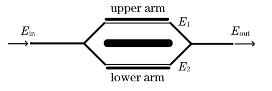
    Fig. 1. Structure of Mach-Zehnder interferometer (MZI)
    Relationship between input and output powers of each signal component in MWP link[13]
    Fig. 2. Relationship between input and output powers of each signal component in MWP link[13]
    Dual-tone test output RF spectrum of MWP link[13]
    Fig. 3. Dual-tone test output RF spectrum of MWP link[13]
    Electrical predistortion method[14]
    Fig. 4. Electrical predistortion method[14]
    Structure of polarization linear modulator[18]
    Fig. 5. Structure of polarization linear modulator[18]
    Structure diagram of double polarizer MZM[19]
    Fig. 6. Structure diagram of double polarizer MZM[19]
    Dual polarization parallel MZM modulator[21]. (a) Model schematic; (b) RF output power as a function of RF input power for dual-polarization modulator and traditional ODSB schemes
    Fig. 7. Dual polarization parallel MZM modulator[21]. (a) Model schematic; (b) RF output power as a function of RF input power for dual-polarization modulator and traditional ODSB schemes
    Dual parallel MZI modulator based on polarization multiplexing[22]. (a) Model schematic; (b) SFDR performance of multi-octave linearized link based on PM-DPMZM
    Fig. 8. Dual parallel MZI modulator based on polarization multiplexing[22]. (a) Model schematic; (b) SFDR performance of multi-octave linearized link based on PM-DPMZM
    Enhanced linearized analog photonic link[23]. (a) Schematic of enhanced linearity link and working points of sub-MZMs; (b) comparison of frequency spectra for two-tone test, where the left is traditional quadrature-biased link and the right is enhanced linearity link; (c) SFDR curves, where the left is traditional quadrature-biased link and the right is enhanced linearity link
    Fig. 9. Enhanced linearized analog photonic link[23]. (a) Schematic of enhanced linearity link and working points of sub-MZMs; (b) comparison of frequency spectra for two-tone test, where the left is traditional quadrature-biased link and the right is enhanced linearity link; (c) SFDR curves, where the left is traditional quadrature-biased link and the right is enhanced linearity link
    Schematics of double parallel and multistage parallel modulators. (a) Double parallel modulator[24]; (b) multistage parallel modulator[25]
    Fig. 10. Schematics of double parallel and multistage parallel modulators. (a) Double parallel modulator[24]; (b) multistage parallel modulator[25]
    Schematic of proposed linearity analog photonic link based on DPMZM[29]
    Fig. 11. Schematic of proposed linearity analog photonic link based on DPMZM[29]
    Structure diagram and microscopy image of double-parallel silicon MZM[30]
    Fig. 12. Structure diagram and microscopy image of double-parallel silicon MZM[30]
    Schematic of single integrated multiplex MZI modulator[31]
    Fig. 13. Schematic of single integrated multiplex MZI modulator[31]
    Dual parallel MZM modulator based on phase shift[32]
    Fig. 14. Dual parallel MZM modulator based on phase shift[32]
    Schematic of series linearized modulator[33]
    Fig. 15. Schematic of series linearized modulator[33]
    Schematic and microscopy image of silicon double series MZM[34]. (a) Schematic; (b) microscopy image
    Fig. 16. Schematic and microscopy image of silicon double series MZM[34]. (a) Schematic; (b) microscopy image
    Structure diagram of micro-ring resonator
    Fig. 17. Structure diagram of micro-ring resonator
    Structure diagram of RAMZM
    Fig. 18. Structure diagram of RAMZM
    Schematic of a RAMZM with push-pull operation[36]
    Fig. 19. Schematic of a RAMZM with push-pull operation[36]
    Two different configurations of IMPACC[37]
    Fig. 20. Two different configurations of IMPACC[37]
    CMOS compatible silicon microring-assisted MZM[38]. (a) Schematic of fabricated ring-assisted MZI modulator;(b) cross-section of waveguide; (c) top-view of fabricated modulator
    Fig. 21. CMOS compatible silicon microring-assisted MZM[38]. (a) Schematic of fabricated ring-assisted MZI modulator;(b) cross-section of waveguide; (c) top-view of fabricated modulator
    Optimized double microring assisted modulator[39]. (a) Microscopic image; (b) measured SFDR curves at 1 GHz and 10 GHz
    Fig. 22. Optimized double microring assisted modulator[39]. (a) Microscopic image; (b) measured SFDR curves at 1 GHz and 10 GHz
    Process flow of heterogeneous-integrated MZM on silicon[40]. (a) Si-WG etch; (b) materials bonding; (c) Ⅲ-Ⅴ etch and N-contact; (d) metallization
    Fig. 23. Process flow of heterogeneous-integrated MZM on silicon[40]. (a) Si-WG etch; (b) materials bonding; (c) Ⅲ-Ⅴ etch and N-contact; (d) metallization
    Structure and technological process of heterogeneous RAMAM on silicon[41]
    Fig. 24. Structure and technological process of heterogeneous RAMAM on silicon[41]
    Reconfigurable silicon RAMZM[12]. (a) Model schematic; (b) modulator chip packaged with a PCB
    Fig. 25. Reconfigurable silicon RAMZM[12]. (a) Model schematic; (b) modulator chip packaged with a PCB
    Compact thin-film lithium niobate electro-optic modulator on silicon[47]. (a) 1550 nm TE field; (b) 10 GHz RF field
    Fig. 26. Compact thin-film lithium niobate electro-optic modulator on silicon[47]. (a) 1550 nm TE field; (b) 10 GHz RF field
    Si/LiNbO3 hybrid ring modulator[48]. (a) Structure diagram; (b) cross-section of device; (c) top-view optical micrograph of fabricated device; (d) SEM image of electrodes
    Fig. 27. Si/LiNbO3 hybrid ring modulator[48]. (a) Structure diagram; (b) cross-section of device; (c) top-view optical micrograph of fabricated device; (d) SEM image of electrodes
    Structure schematic of Si/LiNbO3 hybrid MZM[49]
    Fig. 28. Structure schematic of Si/LiNbO3 hybrid MZM[49]
    FrequencyAmplitude
    ω12I0J0m1J1m2
    ω22I0J0m2J1m1
    2ω1ω22I0J1m1J2m2
    2ω2ω12I0J1m2J2m1
    3ω12I0J0m2J3m1
    3ω22I0J0m1J3m2
    Table 1. Frequency and corresponding amplitude of dual-tone signal
    Processing domainLinearization methodBasic principleAdvantageShortage
    Electrical domainElectronic predistortionIntroducing arcsine predistortion signal to RF signal

    1) Simple operation

    2) Widely applicable

    1) High-speed electronic devices are required to accurately control distortion signals
    Post compensationA specific digital sampling method is used to cancel the distortion at the outputOnly consider electronics problems2) Vulnerable to temperature drift and other unstable factors
    Optical domainDual polarization controlControl the third-order distortion power of TE and TM light at same strength but opposite direction to cancel each otherFundamentally solve the nonlinear problem of light in modulator

    1) It needs to precisely control the distribution of different polarization powers

    2) Structure and control are complex

    MZM series/parallelUsing one MZM to compensate the other one

    1) Wide optical band-width

    2) High manufacturing and temperature tolerance

    1) High optical loss

    2) Structure is relatively complex

    3) Additional compensation

    Microring-assisted MZM (RAMZM)The superlinear phase modulation of the microring and the nonlinear cosine function caused by MZM can cancel each other

    1) Simple structure design

    2) High linearity can be achieved

    1) Low manufacturing tolerance

    2) Linearity is affected by the loss of microring

    Table 2. Common methods for linearization of electrooptical modulator
    ReferenceStructureInsertion loss /dBIMD3 decrement /dBFloor noise /(dBm·Hz-1)SFDRIMD3/dB·Hz2/3
    [11]Silicon microring6-16884@1 GHz
    [50]Silicon MZM6.7-16596.3@1 GHz
    [23]PM-DPMZM25.1-163.1112.3@19 GHz
    [31]PM-DPMZM (control RF)6

    33.7@15 GHz

    30.5@20 GHz

    -162

    110.8@15 GHz

    109.5@20 GHz

    [32]DPMZM (control bias)45-170116.8@12 GHz(simulation)
    [34]MZM series8

    -156@1 GHz

    -152@10 GHz

    109.5@1 GHz

    100.5@10 GHz

    [39]Double-ring RAMZM29-160

    106@1 GHz

    99@10 GHz

    [12]Tunable RAMZM540-163111.3@1 GHz
    [41]Heterogeneous RAMZI5-60117.5@1 GHz
    [47]LNOI MZM-150

    97.3@1 GHz

    92.6@10 GHz

    [49]Si/LiNbO3 hybrid MZM2.5-160

    99.6@1 GHz

    95.2@10 GHz

    [51]LNOI RAMZM10.5

    -163.8@1 GHz

    -162.6@5 GHz

    120.04@1 GHz

    114.54@5 GHz

    Table 3. Performance parameters of different modulator structures
    Zixi Liu, Cheng Zeng, Jinsong Xia. Research Progress on High-Linearity Electro-Optical Modulators[J]. Chinese Journal of Lasers, 2022, 49(12): 1206001
    Download Citation