• Photonics Research
  • Vol. 6, Issue 5, B13 (2018)
Ming Li1, Lin Zhang2, Li-Min Tong1, and Dao-Xin Dai1、*
Author Affiliations
  • 1Centre for Optical and Electromagnetic Research, JORCEP, State Key Laboratory for Modern Optical Instrumentation, Zhejiang Provincial Key Laboratory for Sensing Technologies, Zhejiang University, Hangzhou 310058, China
  • 2Key Laboratory of the Ministry of Education on Optoelectronic Information Technology, School of Precision Instruments and Optoelectronics Engineering, Tianjin University, Tianjin 300072, China
  • show less
    DOI: 10.1364/PRJ.6.000B13 Cite this Article Set citation alerts
    Ming Li, Lin Zhang, Li-Min Tong, Dao-Xin Dai. Hybrid silicon nonlinear photonics [Invited][J]. Photonics Research, 2018, 6(5): B13 Copy Citation Text show less
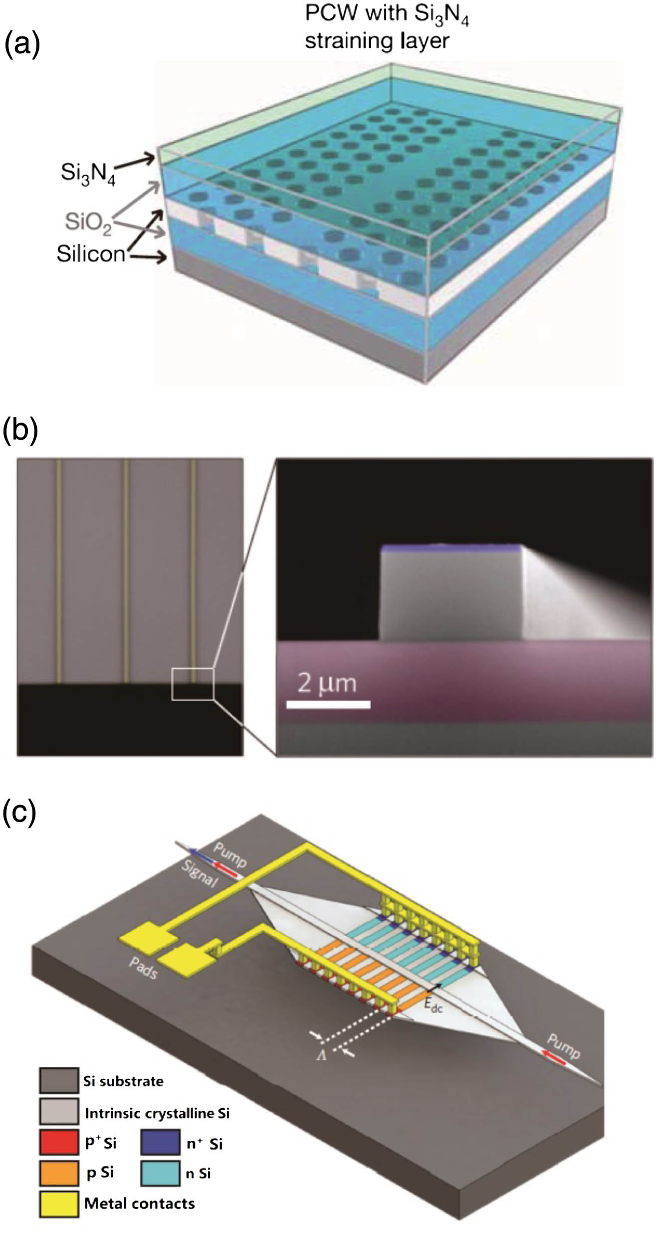
    (a) Diagram of the investigated silicon photonic crystal waveguide with Si3N4 straining layers on top [26]. (b) A top-view optical image of the strained silicon waveguides where a few waveguides are observed as yellow lines. A scanning electron microscopy image of the input facet of the waveguide is also shown. The waveguide is designed to realize second harmonic generation from mid-infrared to near-infrared [28]. (c) Three-dimensional sketch of the electric-field-induced second harmonic generation device with silicon ridge waveguide and spatially periodic patterning of the p–i–n junction. The electric field across the p–i–n junction induces the second-order nonlinear effect in a silicon waveguide. The periodic pattern is designed to alter the nonlinear susceptibility periodically for quasi-phase matching [30].
    Fig. 1. (a) Diagram of the investigated silicon photonic crystal waveguide with Si3N4 straining layers on top [26]. (b) A top-view optical image of the strained silicon waveguides where a few waveguides are observed as yellow lines. A scanning electron microscopy image of the input facet of the waveguide is also shown. The waveguide is designed to realize second harmonic generation from mid-infrared to near-infrared [28]. (c) Three-dimensional sketch of the electric-field-induced second harmonic generation device with silicon ridge waveguide and spatially periodic patterning of the p–i–n junction. The electric field across the p–i–n junction induces the second-order nonlinear effect in a silicon waveguide. The periodic pattern is designed to alter the nonlinear susceptibility periodically for quasi-phase matching [30].
    (a) Schematic of a nanoslot waveguide covered by a nonlinear optical organic material. (b) Experimental setup of the all-optical demultiplexing by four-wave mixing. Inset: 1, diagram of the 170.8 Gb/s data signal; 2, diagram of the 42.7 GHz pump; 3, the spectrum at the output of the DUT (green) and after bandpass-filtering (blue); 4, diagram of the demultiplexed 42.7 Gb/s signal [7].
    Fig. 2. (a) Schematic of a nanoslot waveguide covered by a nonlinear optical organic material. (b) Experimental setup of the all-optical demultiplexing by four-wave mixing. Inset: 1, diagram of the 170.8  Gb/s data signal; 2, diagram of the 42.7 GHz pump; 3, the spectrum at the output of the DUT (green) and after bandpass-filtering (blue); 4, diagram of the demultiplexed 42.7  Gb/s signal [7].
    (a) Schematic of a freestanding nanowire evanescently coupled with integrated silicon waveguide. (b) SEM image of the MZI consisting of a U-shaped 300 nm wide silicon waveguide and a 950 nm diameter CdS free-standing nanowire. The inset shows a close-up view of the right-hand coupling region. (c) Optical micrograph of the integrated nanowire–silicon resonators under a 976 nm wavelength excitation from a tapered fiber probe [70].
    Fig. 3. (a) Schematic of a freestanding nanowire evanescently coupled with integrated silicon waveguide. (b) SEM image of the MZI consisting of a U-shaped 300 nm wide silicon waveguide and a 950 nm diameter CdS free-standing nanowire. The inset shows a close-up view of the right-hand coupling region. (c) Optical micrograph of the integrated nanowire–silicon resonators under a 976 nm wavelength excitation from a tapered fiber probe [70].
    (a) Schematic design of the hybrid integration of MoSe2 onto a silicon waveguide for second harmonic generation (left). Emission spectrum when excited from grating and free space (right) [80]. (b) Scanning electron micrograph of the fabricated silicon photonic crystal cavity with monolayer WSe2 on top, indicated by the orange outline. Visible stripes of holes inside the monolayer region are due to the ripped monolayer during exfoliation (left). The spectrum of the second harmonic waves (right) [84]. (c) Scanning electron micrograph of the tuned photonic crystal cavity (left). Steady-state input/output optical bistability for the quasi-TE cavity mode with laser-cavity (right) [88].
    Fig. 4. (a) Schematic design of the hybrid integration of MoSe2 onto a silicon waveguide for second harmonic generation (left). Emission spectrum when excited from grating and free space (right) [80]. (b) Scanning electron micrograph of the fabricated silicon photonic crystal cavity with monolayer WSe2 on top, indicated by the orange outline. Visible stripes of holes inside the monolayer region are due to the ripped monolayer during exfoliation (left). The spectrum of the second harmonic waves (right) [84]. (c) Scanning electron micrograph of the tuned photonic crystal cavity (left). Steady-state input/output optical bistability for the quasi-TE cavity mode with laser-cavity (right) [88].
    (a) Schematic picture of an in-plane all-optical modulation in graphene-on-silicon suspended membrane waveguides (left). Pump output power at 100 kHz at different input powers (right) [76,77]. (b) Three-dimensional schematic illustration of a graphene-silicon hybrid nanophotonic wire. The probe light is coupled into and out of the silicon-on-insulator (SOI) nanowire by using grating couplers with adiabatic tapers. The pump light is emitted through a fiber on top of the SOI-nanowire (up). Dynamic responses of the output power for TE- and TM-polarization modes of hybrid nanophotonic wires with a locally modulated optical pump (down) [78].
    Fig. 5. (a) Schematic picture of an in-plane all-optical modulation in graphene-on-silicon suspended membrane waveguides (left). Pump output power at 100 kHz at different input powers (right) [76,77]. (b) Three-dimensional schematic illustration of a graphene-silicon hybrid nanophotonic wire. The probe light is coupled into and out of the silicon-on-insulator (SOI) nanowire by using grating couplers with adiabatic tapers. The pump light is emitted through a fiber on top of the SOI-nanowire (up). Dynamic responses of the output power for TE- and TM-polarization modes of hybrid nanophotonic wires with a locally modulated optical pump (down) [78].
    (a) Optical image of bulk (greenish region) and monolayer MoTe2 (contoured region) on PMMA. (b) Scanning electron micrograph of an undercut silicon nanobeam cavity. The dimensions of the nanobeam cavity are 7.2 μm long, 0.365 μm wide, and 0.22 μm thick. The tightly confined mode in the nanocavity ensures the strong coupling between the layered materials and photons. (c) Left: PL spectra of the nanobeam laser with increasing pump power levels at room temperature, which corresponds to an estimated spectral resolution of 0.41 nm. Right: The log–log plot of light in versus light out for two cavity modes and for a background spontaneous emission shows a clear transition from the spontaneous emission to eventual lasing [83].
    Fig. 6. (a) Optical image of bulk (greenish region) and monolayer MoTe2 (contoured region) on PMMA. (b) Scanning electron micrograph of an undercut silicon nanobeam cavity. The dimensions of the nanobeam cavity are 7.2 μm long, 0.365 μm wide, and 0.22 μm thick. The tightly confined mode in the nanocavity ensures the strong coupling between the layered materials and photons. (c) Left: PL spectra of the nanobeam laser with increasing pump power levels at room temperature, which corresponds to an estimated spectral resolution of 0.41 nm. Right: The log–log plot of light in versus light out for two cavity modes and for a background spontaneous emission shows a clear transition from the spontaneous emission to eventual lasing [83].
    MaterialType of Nonlinearity (χ(2), χ(3), etc.)Value (SI Unit)Structure [Waveguide (W), Cavity (C)]Application
    Graphene [7679]χ(3), absorptionχ(3)=3.25×10¹⁹W, CPhase/absorption modulation, bistability
    MoSe2 [80]χ(2)χ(2)=5×10¹¹WSHG
    MoS2 [81,82]χ(2), χ(3)χ(2)=107, χ(3)=2.9×10¹⁹W, CSPM, laser
    MoTe2 [83]CLaser
    WSe2 [84,85]χ(2)χ(2)=6×10¹¹CSHG, laser
    Table 1. Reported Layered Materials for Nonlinear Silicon Photonics
    Ming Li, Lin Zhang, Li-Min Tong, Dao-Xin Dai. Hybrid silicon nonlinear photonics [Invited][J]. Photonics Research, 2018, 6(5): B13
    Download Citation