National Laboratory of Solid State Microstructures, Collaborative Innovation Center of Advanced Microstructures, and College of Engineering and Applied Sciences, Nanjing University, Nanjing 210093, China
In this paper, we present the finding that periodic structural defects (PSDs) along a Bragg grating can shift the Bragg wavelength. This effect is theoretically analyzed and confirmed by numerical calculation. We find that the Bragg wavelength shift is determined by the defect size and the period of the defects. The Bragg wavelength can be well tuned by properly designing the PSDs, and this may provide an alternative method to fabricate grating-based multiwavelength devices, including optical filter arrays and laser arrays. In regards to wavelength precision, the proposed method has an advantage over the traditional methods, where the Bragg wavelengths are changed directly by changing the grating period. In addition, the proposed method can maintain grating strength when tuning the wavelength since only the period of defects is changed. This will be a benefit for devices such as arrays.(BK20130585, BK20140414), the National Natural Science Foundation of China (61435014, 61504170, 61504058), and the National 863 Program (2015AA016902).
Structural defects in photonic crystal (PC) are indispensable elements for almost all PC-based photonic devices. Structural defects can localize the optical mode, which makes the photonic periodic structure functional and versatile. In two-dimensional (2D) PCs, there are basically two types of defects: point defects for resonators and line defects for waveguides. Waveguides and resonators are the building blocks of modern photonics [1–4]. In addition, many other components based on structural defects in PCs have been realized recently, such as optical mirrors, light splitters, optical filters, and even the logic gates for all-optical switching [5–8]. In Bragg gratings, structural defects are also widely applied, such as the narrow bandpass filter based on a phase-shift grating, -phase-shifted distributed feedback (DFB) lasers, and multi-phase-shifted DFB lasers [9–11].
Bragg gratings, the typical 1D PC, have been extensively investigated and are widely employed in many key applications, such as optical filters, semiconductor lasers, optical couplers, and dispersion compensation fibers [9–13]. Usually, the bandgap of PCs is determined by the lattice constant. For Bragg gratings in particular, the Bragg wavelength is fixed by the grating period (), corresponding to , where is the effective refractive index. Then, for grating-based photonic devices in a dense wavelength division multiplexing (DWDM) system, fine-tuning of the wavelength in steps of about 1 nm or less is usually required. Because of the high refractive index of semiconductors in photonic devices, such as Si, In, or P, variation of the grating period with a resolution below the 1 Å range is required, according to the Bragg condition. This is very far below the pixel resolution of lithography systems [14]. Recently, an improved method was developed to equivalently realize the required grating period by alternately stitching two gratings with different periods [15]. The two periods differ in pixel size, which is typically several nanometers [16]. The averaged grating period is between the two periods. However, the tuning range is limited by the difference of the periods and the uniformity of the grating strength. At the middle range of the averaged wavelength, the effective grating strength is reduced. That is to say, the grating strength varies with the wavelength, which will lead to nonuniformity of the whole device.
In this work, we found that the Bragg wavelength shifted when periodic structural defects (PSDs) were introduced along the grating. By adjusting the period and the size of the defects, the wavelength can be well tuned. In this way, to fabricate photonic devices with slightly different Bragg wavelengths, such as multiwavelength laser arrays or grating-based filter arrays for DWDM systems, we do not have to utilize many grating period patterns with slightly different sizes for each wavelength, but can use only two size-fixed patterns, one for the basic uniform grating and one for the defect part.
Sign up for Photonics Research TOC. Get the latest issue of Photonics Research delivered right to you!Sign up now
2. NUMERICAL CALCULATION AND THEORY ANALYSIS
A. Numerical Calculation
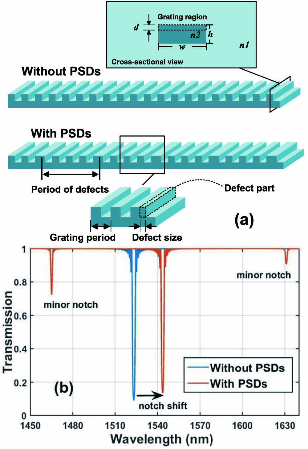
Based on the transmission matrix method (TMM) [17], the spectrum of a Bragg grating with PSDs can be numerically calculated by treating the whole grating as many uniform gratings and defect parts. For a uniform Bragg grating, the transmission spectrum shows a bandgap at the Bragg wavelength, as shown in Fig. 1. By adding PSDs into the uniform grating, the spectrum changes. The transmission notch performs a shift and the depth of the notch decreases slightly. Two minor notches appear at the two sides of the main one. The parameters used in the calculations are listed in Table 1.
Figure 1.(a) Schematic and (b) transmission spectra of the uniform Bragg grating with PSDs and without PSDs.
To investigate the relationship between the defect size and the notch shift, the transmission spectra with different defect sizes are calculated. The relative defect size () is defined as the ratio of defect size () to the grating period (), i.e., . Figure 2 shows the 2D transmission spectrum with the relative defect size changing linearly from to 0.5. The period of defects is fixed at 10 μm, and the other parameters are listed in Table 1. When the relative defect size is not equal to 0, many minor notches appears with approximately the same wavelength spacing and, therefore, are denoted as st order, nd order, etc. The main notch dominates all others and is denoted as the 0th order. As the relative defect size increases, it can be found that the 0th order notch is reduced and other minor ones strengthened. In addition, all the notches shift to the red region when relative defect size is positive and to the blue region when it is negative.
Figure 2.2D transmission spectra when the relative defect size is changed from to 0.5.
We also calculate the 2D transmission spectra with different periods of defects (Fig. 3). The parameters used here are the same as that in Table 1. As the period of defects increases, there are two typical variation trends: one is that the main notch shifts to the blue region, approaching the Bragg wavelength of the basic uniform grating, and the other is that the wavelength spacing between the minor notches decreases.
Figure 3.2D transmission spectra when the period of defects is changed from 1.0 to 10 μm.
To explain this proposed phenomenon, we build a mathematic model. The refractive index of a uniform grating can be described as where is the refractive index modulation, and denotes the longitudinal position. For simplicity, the structural defect is treated as the phase shift of two adjacent uniform gratings. The phase shift formed by the defect can be expressed as . As a consequence, the refractive index of a grating with PSDs can be modeled as Eq. (2), where the stands for the grating phase and can be expressed as Eq. (3), where equals , and is the period of the defects: shows a stair-step-like shape and, as shown in Eq. (4), is equivalent to a superposition of a slope function (before the plus sign) and a periodic sawtooth-like function (after the plus sign). Thus the refractive index of the grating with PSDs can be expanded to a Fourier series in Eq. (5), and we can derive the Fourier series coefficient in Eq. (6):
From Eq. (5), a grating with PSDs is equivalent to a superposition of many uniform subgratings with different grating periods, which are denoted as the 0th, st, nd, etc., orders. The grating period of the th order subgrating is derived by
In particular, the grating period of the 0th-order subgrating is given by which leads to the Bragg wavelength shift. Keeping the parameters used in the calculation of Fig. 3, the wavelength of the 0th-order subgrating is plotted in Fig. 4(a), which is consistent with that in Fig. 3. The grating strength of subgratings is proportional to the absolute value of the coefficient of the Fourier series (), which stands for the refractive index modulation ratio of the subgrating to the uniform grating and is thus called relative grating strength (RGS). The RGS of each subgrating versus the relative defect size is reduced in and is plotted in Fig. 4(b). As the relative defect size increase from 0 to 0.5, the RGS decreases from 1 to 0.61, and that of the st order increases from 0 to 0.61. The RGSs of the other orders increase with the defect size, which are only below 0.2 and can be neglected. In particular, when the relative defect size equals 0.5 (the defect size is equal to the half-grating pitch), the strength of the 0th order is equal to the st-order sub-grating.
Figure 4.(a) Bragg wavelengths of 0 and -order subgratings and (b) the RGS of each order subgrating versus the relative defect size.
Here, we give a physical explanation for the shift of the Bragg wavelength by introducing PSDs, treating the proposed structure as cascade-distributed reflection mirrors. The thickness of each mirror is the distance between two defects (). Supposing that the reflectance and the reflection phase of each mirror are and , respectively, light reflected by the first mirror can be indicated by . Light reflected by the second mirror can be indicated by , where indicates the phase change induced by the first mirror and can be given by , where is the shift of the Bragg wavelength. Consequently, the light reflected by the th mirror can be indicated by . Therefore, by a summation of the whole light reflected by each mirror, one can get the total reflectance () and, hence, the total reflectivity (), which are given, respectively, by
From Eq. (11), one can find that, when and , the reflection of the proposed grating is the same as the uniform one. Moreover, the condition for the main maximum peak is fixed at , and the shift of the Bragg wavelength can consequently be derived as shown in Eq. (12), which is consistent with Eq. (8):
3. APPLICATION TO GRATING-BASED DEVICES WITH WELL-TUNED WAVELENGTHS
A. Lower Fabrication Requirements
When fabricating photonic devices such as multiwavelength Bragg grating arrays [18] and multiwavelength DFB laser arrays [19,20], the common strategy is to adjust the grating pitch to each channel with the help of electron beam lithography (EBL). Taking an eight-channel -phase-shift Bragg grating filter array as an example, half-pitch patterns with eight sizes are required, as illustrated in Fig. 5, instructed by . However, this will lead to very high precision fabrication when the wavelength spacing is small. For example, when the wavelength spacing is about 0.8 nm, the corresponding half-pitch difference is under 1 Å (about 0.06 nm, supposing that is 3.2). This is a challenge for most EBL machines [21]. However, the fabrication is much easier if the wavelength of the grating is tuned by PSDs where only two factors of patterns are required, one for the basic grating and one for the defect part, according to Eq. (8) and Fig. 3. The transmission spectra of an eight-channel -phase-shifted Bragg grating array are calculated in Fig. 6(a). The periods of defects and designed wavelengths are shown in Table 2. As shown in Table 2, one can fabricate a Bragg grating array with 0.8 nm spacing by the proposed method. Thereby, a grating period with 0.13 nm spacing could be equivalently realized.
Figure 5.Comparison of the actual fabrication patterns utilized in an eight-wavelength grating array without PSDs and with PSDs.
Figure 6.(a) Transmission spectra of the PSD-based eight-wavelength -phase-shifted Bragg grating array whose parameters are given in Table 2, and (b) the influence of the DSE.
In actual fabrication, machining error is unavoidable. In EBL, a focused electron beam is used to write the pattern on the photoresist and then transfer the pattern to the wafer by an etching process. Because of the limited writing field, stitching error is inevitable, but it is not considered here. For the grating structure without PSDs, the EBL machine is hard to precisely fabricate the gratings with ultrasmall grating pitch difference when the wavelength spacing is below 0.8 nm [21,22]. As mentioned in [14], the error of wavelength spacing is up to nearly 3 nm.
For the grating structure with PSDs, two kinds of error may have an effect on the wavelength: the defect-size error (DSE) and the defect-period error (DPE). The DSE comes mainly from the pattern transfer process, where a small variation in size is introduced. Then, the defect size is modified to , where is exactly the DSE. As the defect size is much smaller than , typically and μ, Eq. (8) can be Taylor expanded and approximately given by
Then, as implied in Fig. 2, the factor is typically about 0.25. In this condition, the influence of the DSE on the eight-wavelength grating array is calculated and illustrated in Fig. 6(b). Each wavelength shifts to the red region as the defect size increases, and, at the same time, the spacing of two adjacent channels increases slightly. For actual photonic devices, the wavelength spacing and uniformity are more important than the absolute wavelength, because the absolute wavelength of a monolithic grating array can be wholly tuned by heating or cooling, while the spacing and the uniformity have to be adjusted individually after fabrication is complete. Therefore, we utilize spacing change () to characterize the DSE, given by where dP is the defect period difference of adjacent channels. Then we can acquire the error factor , which is typically 0.003, that is to say, 1 nm DSE will lead to wavelength spacing error of only 0.003 nm.
The DPE denotes the fabrication error of the period of defects, . In actual fabrication, the existence of DPE makes each period slightly different from the intended length, that is to say, the is negative or positive near zero. Here we consider the worst situation that all are the same sign and the same value. Therefore, the wavelength error can be derived and denoted by the error factor () in
Typically, the error factor is about 0.0025, which means a 20 nm DPE will bring about a 0.05 nm error of the wavelength in the worst situation. Therefore, the wavelength can be well controlled in the presence of common fabrication error.
C. Comparison with the Grating-Alternated Method
A practical method used in [15] is to stitch two gratings with different periods in a sample unit. The average grating period is tuned by a proper choice of relative contributions of the two constituent gratings. The schematic is shown in the inset of Fig. 7, where is value of the occupation ratio of grating 1, and () is that of grating 2. Thus, the wavelength can be tuned in the range between the Bragg wavelengths of the two gratings. The expression of the averaged grating period is given by where is the averaged grating period. and are the two basic grating periods with a difference of pixel size to reduce fabrication difficulty. However, a critical problem is that the RGS of the averaged grating changes with the occupation ratio, as evidenced by where . Therefore, based on this structure, devices with different wavelengths have different grating strengths. For a grating-based filter array, this may cause different bandwidths, and for a DFB laser array, it may lead to inequality of lasing characteristics. Nevertheless, for devices based on the structure with PSDs, uniformity can be well maintained.
Figure 7.RGS versus occupation ratio of the grating-stitched method. A schematic of a sample unit of the stitched grating is shown in the inset.
Figure 7 plots the calculated RGS of the averaged grating versus the occupation ratio. The and are, respectively, 235 and 245 nm, to ensure enough tuning range, and the pixel size is typically 10 nm [16]. The sample unit length is 6 μm to ensure tuning precision. It can be seen that the RGS is as high as 1 when or and sharply reduces to about 0.6 with approaching 0.5.
D. Laser Static Characteristics
DFB lasers play an important role in the field of optical communication because of their excellent mode selectivity, compact structure, and so on. To investigate the lasing characteristics of DFB lasers with the PSD grating, a spectral domain model is utilized [23]. We simulated the lasing spectrum, the longitudinal light power distribution, and the longitudinal gain distribution of the DFB lasers based on the -phase-shift Bragg gratings with PSDs and without PSDs (traditional structure). The laser parameters modeled in the simulation are listed in Table 3. It can be seen in Fig. 8 that the lasing spectrum of the proposed structure is nearly the same as that of the traditional one. Because of the reduced in the proposed structure, the longitudinal intensity is slightly less and the longitudinal gain is a little higher than that of the traditional case. Roughly speaking, DFB lasers with the proposed structure have almost the same lasing characteristics as traditional DFB lasers. Therefore, the proposed structure with PSDs is a valid method for multiwavelength DFB laser arrays, particularly as applied to a DWDM system.
In this paper, we found that the Bragg wavelength can be shifted when a series of PSDs is introduced along the Bragg grating. The influences of defect size and defect period on the shift of the Bragg wavelength were investigated in detail. The proposed structure can be applied in grating-based multiwavelength devices. As a promising application, a DFB laser with our proposed structure was studied and showed a good consistency with the conventional laser structure. Therefore, a grating with PSDs provides an alternative way to fabricate grating-based photonic devices, such as multiwavelength filter arrays and laser arrays. In addition, the proposed structure can also be applied to other periodic dielectric structures to optimize the characteristic wavelength by designing PSDs.
ACKNOWLEDGMENT
Acknowledgment. This work was supported by the National Natural Science Foundation of China (Youth) (61306068), the Natural Science Foundation of Jiangsu Province of China (BK20130585, BK20140414), the National Natural Science Foundation of China (61435014, 61504170, 61504058), and the National 863 Program (2015AA016902).
References
[1] M. Skorobogatiy, J. Yang. Fundamentals of Photonic Crystal Guiding(2009).
[3] A. Mekis, J. C. Chen, I. Kuiland, S. Fan, P. R. Villeneuve, J. D. Joannopoulos. High transmission through sharp bends in photonic crystal waveguides. Phys. Rev. Lett., 38, 4188-4190(2011).