
Yi Zhao, Qiuping Huang, Honglei Cai, Xiaoxia Lin, Hongchuan He, Hao Cheng, Tian Ma, Yalin Lu. Ultrafast control of slow light in THz electromagnetically induced transparency metasurfaces[J]. Chinese Optics Letters, 2021, 19(7): 073602
- Chinese Optics Letters
- Vol. 19, Issue 7, 073602 (2021)
Abstract
1. Introduction
Electromagnetically induced transparency (EIT) is a quantum interference effect that renders a medium transparent within a narrow spectral range around an absorption line[
For practical applications, it is desirable that the group velocity of electromagnetic waves can be actively controlled. For this purpose, a controllable EIT metasurface is an excellent candidate. Many efforts have been devoted to the tunable EIT metasurfaces[
In this paper, we propose ultrafast tunable slow light metasurfaces based on a bright-bright mode coupling EIT-like structure. The unit cell of the metasurfaces consists of a gold (Au) cut wire (CW) and two Au split-ring resonators (SRRs). In order to achieve ultrafast control of slow light, we integrate -implanted Si CW into the SRRs. Due to the intrinsic Si having a long carrier recombination life time on the order of milliseconds, the Si in our experiments is implanted with to produce lattice defects of Si and further reduce the carrier lifetime of Si. Compared with previous optically tunable EIT metasurfaces[
Sign up for Chinese Optics Letters TOC. Get the latest issue of Chinese Optics Letters delivered right to you!Sign up now
2. Structure Design and Experiments
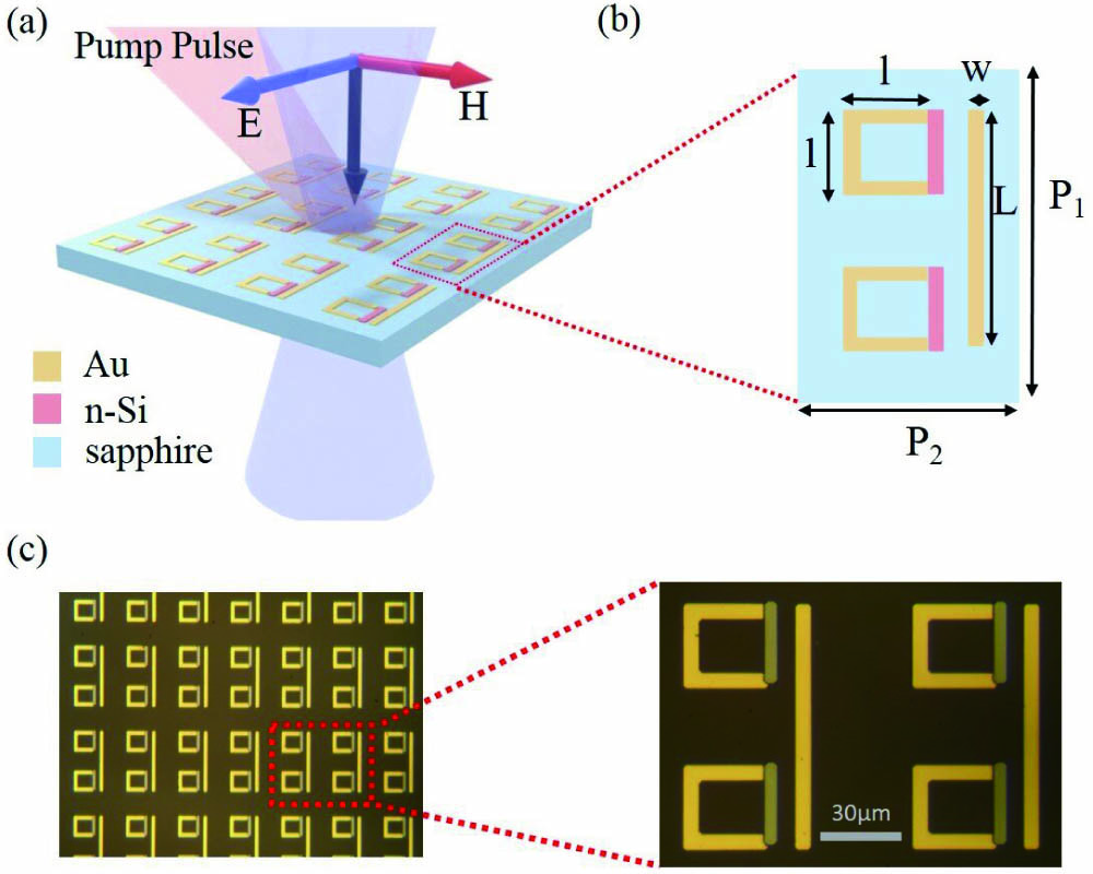
The schematic illustration of the ultrafast EIT metasurface is shown in Figs. 1(a) and 1(b). As shown in Fig. 1(b), the unit cell of the EIT metasurface consists of a CW and two SRRs, which are made of Au, and there is a CW made of between the CW and each SRR. The parameters of the structure are given: the length of Au CW , the width of Au CW and SRR , the side length of SRR , and the periods of the structure , . The size of the unit cell ensures that no diffraction happens, and thus the EIT metasurface behaves as an effective medium. The structure was fabricated on the Si-on-sapphire (SOS) wafer comprised of 600 nm thick Si and 530 μm thick sapphire, with a microscopy image shown in Fig. 1(c). Firstly, the Si layer of SOS was ion implanted with at a dose of and an energy of 100 keV. Then, the CW of Si was fabricated by the standard UV photolithography and reactive ion etching on the SOS substrate. Finally, the Au CW and Au SRRs are overlaid on the Si structure using the lift-off method.
![]()
Figure 1.(a) Schematic of the ultrafast EIT metasurface. (b) Parameters of structure: P1 = 120 µm, P2 = 80 µm, L = 85 µm, w = 5 µm, and l = 29 µm. (c) Microscopy image of the fabricated sample.
3. Results and Discussions
We firstly utilized the commercial software COMSOL Multiphysics 5.2 to simulate the transmission spectra. In our simulation, the propagation of the incident electromagnetic wave is perpendicular to the surface of the structure, while the (E, H) plane is parallel to the surface of the structure, as shown in Fig. 1(a). The incident wave is generated by the port boundary conditions (in our simulation, the power of the incident wave is 1 W, and the absolute value of the corresponding electric field intensity can be calculated as ), and the periodic boundary conditions are employed. The transmission coefficient can be obtained from the simulations, and the transmission T is extracted by . In our simulation, the sapphire substrate was treated as a lossless dielectric with [
![]()
Figure 2.(a) Simulated transmission spectra of Au CW, Au SRRs, and EIT sample, respectively. Electric field distribution of (b) Au SRRs at 0.89 THz and (c) Au CW at 0.7 THz. (d) Simulated transmission spectra of the EIT metasurface with different Si conductivity. Electric field distributions at 0.76 THz when Si conductivity is (e) 200 S/m and (f) 60,000 S/m (in our simulation, the absolute value of the electric field intensity of the incident wave is 2.8 × 10⁵ V/m).
Then, we characterized the fabricated EIT metasurface by a homemade OPTP spectrometer, with the experimental setup described in detail elsewhere[
![]()
Figure 3.Schematic illustration of the OPTP system. The ultrafast femtosecond laser beam is split into three beams, respectively, used for THz generation, THz detection, and ultrafast optical pump.
The differential change in the transmitted THz peak signal () was measured as a function of pump–probe delay, with the results shown in Fig. 4(a). It can be seen that the THz peak signal firstly reduces rapidly, resulting from the photogenerated carriers in the Si CW. Until the time delay reaches 5 ps, the THz peak signal starts to recover due to the recombination of carriers in Si. It can return to be the initial state within 200 ps. Additionally, the transmission spectra of the EIT metasurface at different pump–probe delays are shown in Fig. 4(b). When the time delay is , there is no photoexcitation, and the corresponding transmission spectra show an EIT peak at 0.78 THz, while the EIT peak is totally suppressed when the time delay reaches 5 ps. As the time delay increases from 5 ps to 180 ps, the EIT peak appears again. One cycle of switching from the EIT suppressing to the EIT reappearing takes within 200 ps.
![]()
Figure 4.(a) Differential change in transmitted THz peak signal as a function of pump–probe delay. Black dots indicate the specific time delay of our test. (b) Experimental transmission spectra at different time delays. (c) Time-dependent Δtg retrieved from measured transmission spectra. (d) Time-dependent Δtg at 0.78 THz.
In the following, ultrafast modulation of the slow light behavior is further demonstrated. The EIT metasurface changes the group refractive index by changing the dispersion of the metasurface. Since the increasing group refractive index increases the time of THz waves passing through the metasurface, the slow light effect of the metasurface can be characterized by this time value. Therefore, we use to describe the slow light capability of our device[
Experimental transmission spectrum mapping as a function of pump–probe time delay is shown in Fig. 5(a) to more clearly illustrate the switching characteristics of the device. As indicated by the dashed black line, one cycle of switching on and switching off the EIT peak is within 200 ps. Additionally, to illustrate the effect of ion implantation on carrier lifetime and thus the manipulation speed of the EIT metasurface, we measured the differential change of the transmitted THz peak signal for different Si films with doping doses of , , and but annealed (rapid thermal annealing at 1000°C for 30 s), respectively. The transient differential transmission trace is fitted by a single exponential expression , and the relaxation time is obtained, as shown in Fig. 5(b). The sample with an implantation dose of and without annealing presents a shorter relaxation time but a lower modulation depth than that of the implanted Si film and without annealing. This is due to a higher implantation dose that results in more crystal defects, which heavily reduces the carrier lifetime of Si. However, the annealing post-procession can repair the crystal defects and activate the implanted , thus improving the carrier density and extending the carrier lifetime. So, the annealing sample has a much higher modulation depth, but much longer relaxation time. Therefore, in our experiment, a Si film with a doping dose of but without annealing was selected to fabricate the metasurface, taking into account that it has a good modulation depth and also a relatively short carrier lifetime.
![]()
Figure 5.(a) Experimental transmission spectrum mapping as a function of pump–probe delay. (b) Differential change in transmitted THz peak signal as a function of pump–probe delay for Si films with different implanted conditions. The solid curve represents the single exponential fitting with a time constant of τ.
To explain the physical origin of the EIT behavior, we use the coupled oscillator model[
The electric current density and the surface conductivity of the metasurface can be expressed as
The transmission coefficients of the metasurface can be calculated from Eq. (6):
The simulated transmission spectra with Si conductivity that varied between 200 S/m and 60,000 S/m are presented by red dotted line in Figs. 6(a)–6(e). When the Si conductivity is set to be 200 S/m, the EIT peak is activated, similar to the experimental result at in Fig. 4(b). The EIT phenomenon is suppressed when the Si conductivity increases to 60,000 S/m, which is the same as the experimental one at 5 ps. Therefore, it can be concluded that the ultrafast manipulation of carrier density of Si CW and thus conductivity of Si contributed to the ultrafast control of the EIT peak.
![]()
Figure 6.(a)–(e) Simulated transmission spectra with Si conductivity varied between 200 S/m and 60,000 S/m (red dots) and the corresponding fitting lines (black lines). (f) The fitted parameters with different Si conductivity.
The equation of is used to fit the simulation results in Figs. 6(a)–6(e), with fitted results shown by black lines in Figs. 6(a)–6(e). The fitting parameters with the Si conductivity are plotted in Fig. 6(f).
As can be seen from Fig. 6(f), and change slightly because the Au CW resonators are hardly affected by the change of Si conductivity. A significant change in and can be seen due to the change of Si conductivity that can affect the damping rate of the SRRs and the effective length of the electric dipole (SRRs). The value of changes a little because the effective distance between these two resonators also varies a little due to the change of Si conductivity. From the above analysis, we can see that the whole process is indeed due to the ultrafast change of Si conductivity, which has a great influence on the SRRs and destroys the interference between the bright-bright mode couplings.
4. Conclusions
In summary, by incorporating -implanted Si CW into the EIT metasurface unit cell, we have experimentally demonstrated an ultrafast dynamic control of slow light in THz metasurfaces. The transition from the state with the slow light effect to the state without the slow light effect occurs at an ultrafast time of 5 ps, and the recovery to the slow light effect state takes 200 ps. A coupled oscillator model has been used to explain the origin of the controllability. The ultrafast manipulation of conductivity of Si CW affects the damping rate and the effective electric dipole length of the SRRs, and thus destroys the interference between the bright-bright mode couplings. The structure we designed may be applied to an ultrafast THz band optical delay device.
References
[1] K. J. Boller, A. Imamoğlu, S. E. Harris. Observation of electromagnetically induced transparency. Phys. Rev. Lett., 66, 2593(1991).
[2] Q. Xu, S. Sandhu, M. L. Povinelli, J. Shakya, S. Fan, M. Lipson. Experimental realization of an on-chip all-optical analogue to electromagnetically induced transparency. Phys. Rev. Lett., 96, 123901(2006).
[3] X. Yang, M. Yu, D.-L. Kwong, C. W. Wong. All-optical analog to electromagnetically induced transparency in multiple coupled photonic crystal cavities. Phys. Rev. Lett., 102, 173902(2009).
[4] C. L. Garrido Alzar, M. A. G. Martinez, P. Nussenzveig. Classical analog of electromagnetically induced transparency. Am. J. Phys., 70, 37(2002).
[5] S. Zhang, D. A. Genov, Y. Wang, M. Liu, X. Zhang. Plasmon-induced transparency in metamaterials. Phys. Rev. Lett., 101, 047401(2008).
[6] N. Papasimakis, V. A. Fedotov, N. Zheludev, S. Prosvirnin. Metamaterial analog of electromagnetically induced transparency. Phys. Rev. Lett., 101, 253903(2008).
[7] X. Liu, J. Gu, R. Singh, Y. Ma, J. Zhu, Z. Tian, M. He, J. Han, W. Zhang. Electromagnetically induced transparency in terahertz plasmonic metamaterials via dual excitation pathways of the dark mode. Appl. Phys. Lett., 100, 131101(2012).
[8] N. Verellen, Y. Sonnefraud, H. Sobhani, F. Hao, V. V. Moshchalkov, P. V. Dorpe, P. Nordlander, S. A. Maier. Fano resonances in individual coherent plasmonic nanocavities. Nano Lett., 9, 1663(2009).
[9] Y. Francescato, V. Giannini, S. A. Maier. Plasmonic systems unveiled by Fano resonances. ACS Nano, 6, 1830(2012).
[10] G. Heinze, C. Hubrich, T. Halfmann. Stopped light and image storage by electromagnetically induced transparency up to the regime of one minute. Phys. Rev. Lett., 111, 033601(2013).
[11] T. F. Krauss. Why do we need slow light?. Nat. Photon., 2, 448(2008).
[12] D. M. Beggs, T. P. White, L. O’Faolain, T. F. Krauss. Ultracompact and low-power optical switch based on silicon photonic crystals. Opt. Lett., 33, 147(2008).
[13] M. Lee, M. E. Gehm, M. A. Neifeld. Systematic design study of an all-optical delay line based on Brillouin scattering enhanced cascade coupled ring resonators. J. Opt., 12, 104012(2010).
[14] S. Savo, B. Casse, W. Lu, S. Sridhar. Observation of slow-light in a metamaterials waveguide at microwave frequencies. Appl. Phys. Lett., 98, 171907(2011).
[15] K. L. Tsakmakidis, A. D. Boardman, O. Hess. Trapped rainbow’ storage of light in metamaterials. Nature, 450, 397(2007).
[16] L. Zhang, P. Tassin, T. Koschny, C. Kurter, S. M. Anlage, C. M. Soukoulis. Large group delay in a microwave metamaterial analog of electromagnetically induced transparency. Appl. Phys. Lett., 97, 241904(2010).
[17] C. Wu, A. B. Khanikaev, G. Shvets. Broadband slow light metamaterial based on a double-continuum Fano resonance. Phys. Rev. Lett., 106, 107403(2011).
[18] J. Zhang, S. Xiao, C. Jeppesen, A. Kristensen, N. A. Mortensen. Electromagnetically induced transparency in metamaterials at near-infrared frequency. Opt. Express, 18, 17187(2010).
[19] C. Kurter, P. Tassin, L. Zhang, T. Koschny, A. P. Zhuravel, A. V. Ustinov, S. M. Anlage, C. M. Soukoulis. Classical analogue of electromagnetically induced transparency with a metal-superconductor hybrid metamaterial. Phys. Rev. Lett., 107, 043901(2011).
[20] W. Cao, R. Singh, C. Zhang, J. Han, M. Tonouchi, W. Zhang. Plasmon-induced transparency in metamaterials: active near field coupling between bright superconducting and dark metallic mode resonators. Appl. Phys. Lett., 103, 101106(2013).
[21] J. Gu, R. Singh, X. Liu, X. Zhang, Y. Ma, S. Zhang, S. A. Maier, Z. Tian, A. K. Azad, H.-T. Chen. Active control of electromagnetically induced transparency analogue in terahertz metamaterials. Nat. Commun., 3, 1151(2012).
[22] F. Miyamaru, H. Morita, Y. Nishiyama, T. Nishida, T. Nakanishi, M. Kitano, M. W. Takeda. Ultrafast optical control of group delay of narrow-band terahertz waves. Sci. Rep., 4, 4346(2014).
[23] S. Xiao, T. Wang, T. Liu, X. Yan, Z. Li, C. Xu. Active modulation of electromagnetically induced transparency analogue in terahertz hybrid metal-graphene metamaterials. Carbon, 126, 271(2018).
[24] T. T. Kim, H. D. Kim, R. Zhao, S. O. Sang, T. Ha, D. Chung, Y. H. Lee, B. Min, Z. Shuang. Electrically tunable slow light using graphene metamaterials. ACS Photon., 5, 1800(2018).
[25] Y. Hu, J. You, M. Tong, X. Zheng, Z. Xu, X. Cheng, T. Jiang. Pump‐color selective control of ultrafast all‐optical switching dynamics in metaphotonic devices. Adv. Sci., 2000799(2020).
[26] H. Sun, J. Yang, H. Liu, D. Wu, X. Zheng. Process-controllable modulation of plasmon-induced transparency in terahertz metamaterials. Chin. Opt. Lett., 19, 013602(2021).
[27] H. Sun, Y. Tang, Y. Hu, J. You, H. Liu, X. Zheng. Active formatting modulation of electromagnetically induced transparency in metamaterials. Chin. Opt. Lett., 18, 092402(2020).
[28] M. A. Ordal, L. L. Long, R. J. Bell, S. E. Bell, R. R. Bell, R. W. Alexander, C. A. Ward. Optical properties of the metals Al, Co, Cu, Au, Fe, Pb, Ni, Pd, Pt, Ag, Ti, and W in the infrared and far infrared. Appl. Opt., 22, 1099(1983).
[29] N. Kamaraju, A. Rubano, L. Jian, S. Venkatesan. Subcycle control of terahertz wave form polarization using all-optically induced transient metamaterials. Light: Sci. Appl., 3, e155(2014).
[30] K. Sokolowskitnten, D. V. der Linde. Generation of dense electron-hole plasmas in silicon. Phys. Rev. B, 61, 2643(2000).
[31] H. Cai, S. Chen, C. Zou, Q. Huang, Y. Liu, X. Hu, Z. Fu, Y. Zhao, H. He, Y. Lu. Multifunctional hybrid metasurfaces for dynamic tuning of terahertz waves. Adv. Opt. Mater., 6, 1800257(2018).
[32] W. Withayachumnankul, B. M. Fischer, B. Ferguson, B. R. Davis, D. Abbott. A systemized view of superluminal wave propagation. Proc. IEEE, 98, 1775(2010).
[33] X. Hu, S. Yuan, A. Armghan, Y. Liu, Z. Jiao, H. Lv, C. Zeng, Y. Huang, Q. Huang, Y. Wang, J. Xia. Plasmon induced transparency and absorption in bright–bright mode coupling metamaterials: a radiating two-oscillator model analysis. J. Phys. D: Appl. Phys., 50, 025301(2016).

Set citation alerts for the article
Please enter your email address
© Copyright 2018-2021 | Chinese Laser Press. All Rights Reserved 沪ICP备15018463号-20