
Dezhong Cao, Xiaokun Yang, Lüyang Shen, Chongchong Zhao, Caina Luan, Jin Ma, Hongdi Xiao, "Fabrication and properties of high quality InGaN-based LEDs with highly reflective nanoporous GaN mirrors," Photonics Res. 6, 1144 (2018)
- Photonics Research
- Vol. 6, Issue 12, 1144 (2018)
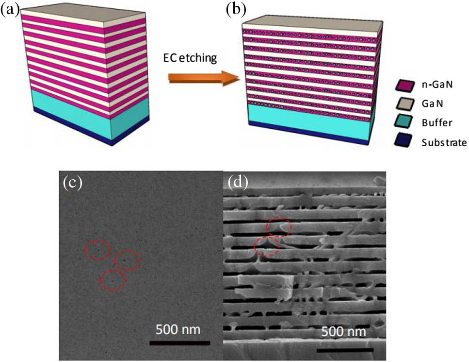
Fig. 1. (a),(b) Schematic for the fabrication of a highly reflective NP-GaN DBR mirror. (a) Epitaxial growth of λ / 4
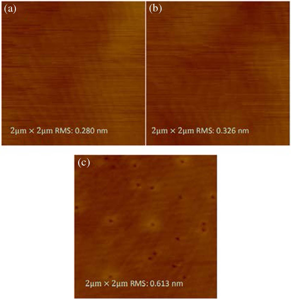
Fig. 2. AFM images taken from (a) as-grown GaN thin film, (b) GaN thin film etched in 0.3 M NaNO 3
Fig. 3. (a) Reflectance from the NP-GaN DBR in the blue wavelength region; (b) photograph of a 20.3 cm2 NP-GaN DBR wafer reflecting a card with the Shandong University logo. In (b), the original logo is reddish brown rather than black, which should be related to the shooting angle of the camera.
Fig. 4. (a) Photograph of an LED with a 1.9 μm Si-doped n-GaN layer (1050°C); (b) photograph of an LED sample with double n-GaN layers consisting of a 400 nm Si-doped n-GaN layer (900°C) and followed by a 1.5 μm Si-doped n-GaN layer (1050°C); (c) reflectance from the reference LED and the LED with DBRs shown in (b).
Fig. 5. (a) Cross-sectional SEM image of the InGaN-based LED regrown on the DBRs. AFM images of regrown InGaN-based LEDs (b) without and (c) with the DBRs; (d) HRXRD patterns of the InGaN-based LEDs, and (e) XRD rocking curves using (0002) diffractions for the LEDs.
Fig. 6. (a) LED structures for room-temperature PL spectra (solid line) and reflectance spectrum (dotted line); (b) Voigt fitting curves (dotted line) of PL peaks shown in (a), and (c) TCSPC measurement.
Fig. 7. (a) I-V characteristics and (b) room-temperature EL spectra and optical image at a 5 mA current injection.


Set citation alerts for the article
Please enter your email address

© Copyright 2018-2021 | Chinese Laser Press. All Rights Reserved 沪ICP备15018463号-20