Abstract
Distributed Bragg reflectors (DBRs) are essential components for the development of optoelectronic devices. In this paper, we first report the use of the nanoporous GaN (NP-GaN) DBR as a template for regrowth of InGaN-based light-emitting diodes (LEDs). The wafer-scale NP-GaN DBR, which is fabricated by electrochemical etching in a neutral solution, has a smooth surface, high reflectivity (), and wide spectral stop band width (). The chemical composition of the regrown LED thin film is similar to that of the reference LED, but the photoluminescence (PL) lifetime, PL intensity, and electroluminescence intensity of the LED with the DBR are enhanced several times compared to those of the reference LED. The intensity enhancement is attributed to the light reflection effect of the NP-GaN DBR and improved crystalline quality as a result of the etching scheme, whereas the enhancement of PL lifetime is attributable to the latter.1. INTRODUCTION
Distributed Bragg reflectors (DBRs) with minimum absorption and high reflectivity have been considered as essential components of optical devices such as resonant-cavity light-emitting diodes (RCLEDs) [1–3] and vertical-cavity surface emitting laser diodes (VCSELs) [4–6]. Compared to the GaAs/AlGaAs DBR material system with mature technology [7], the fabrication of GaN/(Ga,Al,In)N DBRs is still one of the most challenging topics in III-nitride materials research after two decades of endeavors. The challenge is mainly the lack of material pairs with marked contrast of refractive indices, low strain accumulation, and good crystalline quality [8–12].
Research on GaN/nanoporous GaN (NP-GaN) DBRs that can solve the above-mentioned problem has drawn much attention [13–16]. At present, a vast amount of literature exists on the fabrication of GaN/NP-GaN DBRs by a laterally electrochemical (EC) etching method using toxic acids such as HF, , and oxalic acid [16–18]. Because the laterally EC etching length is usually shorter than 50 μm, it is difficult to fabricate a large-area GaN/NP-GaN DBR structure [16–18]. Compared to InGaN-based LEDs regrown on sapphire substrates, the LEDs embedded on the GaN/NP-GaN DBRs via lateral EC etching only present a twofold enhancement in the photoluminescence (PL) intensity [19], which is even lower than the enhancement value (3 times) of the LEDs regrown on NP-GaN templates [20]. Supposing that the LEDs are regrown on the GaN/NP-GaN DBR templates, the LEDs should present a higher light-emitting efficiency. Having a large surface area, however, NP-GaN is energetically unstable against annealing (Rayleigh instability). Novel configurations and shapes of GaN can be obtained through curvature-driven mass transport at elevated temperatures [15,21]. Based on such a realization, no works were performed on the regrowth of InGaN-based LEDs on the GaN/NP-GaN DBR templates.
In the paper, a wafer-scale GaN/NP-GaN DBR with high reflectivity () was fabricated with one-step EC porosification in a neutral solution for the first time, demonstrating that the above-mentioned harsh etchants are unnecessary. Excellent etching properties were documented for solution that are safe and environmentally friendly. Subsequently, the etched periodic structure acted as a template for the regrowth of an InGaN-based LED. The InGaN-based LED grown on the NP-GaN DBR template presented high quality and high light extraction efficiency.
Sign up for Photonics Research TOC. Get the latest issue of Photonics Research delivered right to you!Sign up now
2. EXPERIMENTS AND MEASUREMENT
A. EC Porosification
Wafer-scale DBRs were prepared via one-step EC etching in a two-electrode cell with an undoped GaN/n-type GaN periodic structure as the anode and a platinum wire as the cathode. The periodic structure comprising 12 pairs of alternating n-GaN with a silicon doping concentration () of and undoped GaN layers was grown on c-plane sapphire with a metal-organic chemical vapor deposition (MOCVD) method. In the structure, the thicknesses of the undoped and n-GaN layers are 50 and 65 nm, respectively. The etching processes were performed at a constant voltage (18 V) for 20 min in 0.3 M (1 M 1 mol/L) solution, controlled by a Gwinstek GPD-3303S source meter under room light. After anodization, samples were rinsed with deionized water and dried in .
B. MOCVD Regrowth of LED Structure
InGaN-based LED thin films were regrown on the as-grown and etched GaN periodic structures using the MOCVD method. The LED structure consisted of a 1.9 μm Si doped n-GaN layer, a 10-period superlattice (SL) epilayer with 3-nm-thick InGaN wells and 7-nm-thick GaN barriers, a 14-period multiple quantum well (MQW) as the active region with 4-nm-thick InGaN wells and 10-nm-thick GaN barriers, and a 280-nm-thick Mg doped p-GaN layer .
C. Material Characterization
Morphology of the samples was characterized with scanning electron microscopy (SEM, JEOL JSM-6700F) and atomic force microscopy (AFM, Dimension Edge, Bruker). Reflectance measurements were performed via a bright-field microscope (BX51, Olympus) connected with a fiber-coupled spectrometer (QE65000, Ocean Optics) using a commercial silver mirror (PF10-03-P01, Thorlabs) for calibration. The structural characterization was done by high-resolution X-ray diffraction (HRXRD, X’Pert PRO and Rigaku X-ray diffractometers) measurements. Room-temperature PL spectroscopy with a He-Cd laser emitting at 325 nm was carried out. The PL lifetime was collected by a time-correlated single-photon counting (TCSPC) setup, using frequency doubling of the output of a Ti:sapphire laser (Maitai HP, Spectra-Physics) (, 80 MHz repetition rate) from PicoQuant and an avalanche photon counting module from the Halcyone spectrometer (Ultrafast System). The measurement error of the spectrometer is about . The data were curve-fitted by Gaussian and exponential convolution methods. To compare electrical properties of the regrown LEDs, wafer probing of the LED structures was done. Current-voltage (I-V) measurements were performed by using an Agilent B1500A semiconductor parameter analyzer, whereas electroluminescence (EL) characteristics at room temperature were evaluated by injecting a dc current into the two LEDs.
3. RESULTS AND DISCUSSION
Figures 1(a) and 1(b) show the schematic diagram of making the NP-GaN DBR mirrors. An epitaxial structure comprising alternating undoped GaN and n-GaN layers is grown. Subsequently, the samples are etched by a one-step EC etching method. Figures 1(c) and 1(d) illustrate the top view and cross-sectional SEM images of the etched sample at 18 V in for 20 min. The etching results in extremely sparse nanopores (marked by red dotted circles) in the undoped GaN layers imply that the EC porosification mechanism should involve a vertical etching component, which may be defect-related [15]. According to previous reports [14], the etching rate and porosity decrease with decreasing of the doping concentration, i.e., the undoped GaN layer should present the slowest etching rate and the lowest porosity. Due to the restriction of the adjacent undoped GaN layers, the etching has to be along the horizontal directions (i.e., lateral etching) and leads to high porosity in the n-GaN layers.
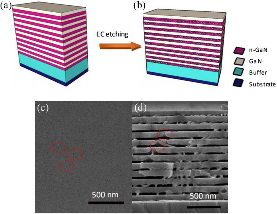
Figure 1.(a),(b) Schematic for the fabrication of a highly reflective NP-GaN DBR mirror. (a) Epitaxial growth of GaN/n-GaN structures; (b) EC etching to form NP-GaN DBR mirror; (c) top view and (d) cross-sectional SEM images of an NP-GaN DBR sample. The dotted circles imply the position where the undoped GaN layers have been etched due to the vertical etching component in the EC porosification process.
To investigate possible etching damage of the NP-GaN DBR structure, AFM images were taken from nonporous and porous regions, which are shown in Fig. 2. Compared to the as-grown GaN periodic structure, the root mean square roughness () of the etched GaN surface presents a slight increase [Figs. 2(a) and 2(b)]. In contrast, this value is much lower than that of an NP-GaN DBR fabricated at 18 V in oxalic acid, as shown in Fig. 2(c). The comparison means that the solution is more suitable for the fabrication of NP-GaN DBR mirrors than the oxalic acid solution.

Figure 2.AFM images taken from (a) as-grown GaN thin film, (b) GaN thin film etched in 0.3 M solution, and (c) GaN thin film etched in 0.3 M oxalic acid solution.
Figure 3(a) shows the measured reflectance spectrum of the NP-GaN DBR mirror. A wide stop band with high reflectance () from 454 to 520 nm is presented across the wafer. The uniformity can be confirmed by the same reflectivity spectra obtained in different areas of the sample. The peak reflectance reported here is higher than that (95%) of the nonpolar (110) mesoporous GaN DBR structure fabricated in oxalic acid [15]. Figure 3(b) shows a photograph of the wafer-scale NP-GaN DBR mirror under room-light illumination and the reflection of a card with a reddish-brown logo. While the unetched region is transparent, the high reflection in the DBR region further demonstrates the uniform EC porosification process.
Figure 3.(a) Reflectance from the NP-GaN DBR in the blue wavelength region; (b) photograph of a 20.3 cm2 NP-GaN DBR wafer reflecting a card with the Shandong University logo. In (b), the original logo is reddish brown rather than black, which should be related to the shooting angle of the camera.
To estimate possible applications, the InGaN-based LEDs were grown on the NP-GaN DBR templates. Figures 4(a) and 4(b) show the photographs of the InGaN-based LED samples grown on the NP-GaN DBR templates presented in Fig. 3(b). The difference in the two samples is focused on the growth temperature of the n-GaN layers of the LEDs. The n-GaN layer in the sample shown in Fig. 4(a) is a 1.9 μm Si-doped n-GaN layer grown at 1050°C. Such a high temperature can lead to the dissociation of the NP-GaN DBR layer, confirmed by the black wafer shown in Fig. 4(a). To protect the NP-GaN DBR structure, a n-GaN layer is grown at 900°C and followed by a 1.5 μm n-GaN layer grown at 1050°C [Fig. 4(b)]. Compared to the NP-GaN DBR mirror shown in Fig. 3(b), the NP-GaN DBR covered by the LED thin film presents not only a lower reflectivity but also light interference signals in the reflectance spectrum [Fig. 4(c)]. The lower reflectivity should be attributable to light absorption of the LED thin film [14], whereas the light interference signal should be a result of the light reflected between the top air/p-GaN and the bottom n-GaN/NP-GaN DBR interferences [22].
Figure 4.(a) Photograph of an LED with a 1.9 μm Si-doped n-GaN layer (1050°C); (b) photograph of an LED sample with double n-GaN layers consisting of a 400 nm Si-doped n-GaN layer (900°C) and followed by a 1.5 μm Si-doped n-GaN layer (1050°C); (c) reflectance from the reference LED and the LED with DBRs shown in (b).
Figure 5(a) shows the cross-sectional SEM image of the LED sample presented in Fig. 4(b). Compared to the NP-GaN DBR shown in Fig. 1(c), the morphology of the DBR after the regrowth presents significant changes (e.g., smooth nanopores) due to mass transport from high-curvature to low-curvature regions [23]. The LED on the NP-GaN DBR, which is called the DBR-LED, exhibits an value of determined from a AFM scan, which is lower than that () of the LEDs grown on the reference template (i.e., the GaN layer is not subjected to etching) [Figs. 5(b) and 5(c)], indicating that the InGaN/GaN interfaces of the DBR-LED have lower density of interface states than those of the reference LED, i.e., the MQW structure grown on the etched template has higher crystalline quality. Furthermore, the microstructural quality of the LEDs without and with the DBR was characterized by the HRXRD [Fig. 5(d)]. The strongest peak in the diffraction pattern is due to the (0002) reflection of the GaN layer in the two samples. The position of the MQW-related satellite peaks is virtually similar, meaning that the indium compositions should be similar in the two tested samples and are not affected by the templates. However, compared to the reference sample, the DBR-LED shows a slightly reduced linewidth of the InGaN (0002) reflection in the rocking curve [Fig. 5(e)], which may be attributed to the “natural” annihilation of dislocations as epitaxy proceeds [23,24].
Figure 5.(a) Cross-sectional SEM image of the InGaN-based LED regrown on the DBRs. AFM images of regrown InGaN-based LEDs (b) without and (c) with the DBRs; (d) HRXRD patterns of the InGaN-based LEDs, and (e) XRD rocking curves using (0002) diffractions for the LEDs.
To study the optical and electrical properties of the regrown LED structures, luminescence measurements were carried out at room temperature. Figure 6(a) shows the room-temperature PL spectra of the regrown LED structures. The peak wavelengths were 463.4 and 464.5 nm for the LEDs without and with the DBR, respectively. Usually, the wavelength difference across the 20.3 cm2 wafer is already more than 1.1 nm. Therefore, the 1.1 nm difference should not be attributed to strain relaxation of the DBR-LED structure. It is also found from Fig. 6(a) that the PL intensity of the wafer-scale DBR-LED presents a fivefold enhancement compared to that of the standard LED. The enhancement value is markedly higher than the recently reported values for the InGaN-based LEDs grown on NP-GaN template with a threefold enhancement [20] and for that embedded on NP-GaN DBR fabricated by lateral EC etching with a twofold enhancement [19]. Therefore, the enhancement in this work should be attributed to increased internal quantum efficiency (IQE) due to the improved crystalline quality [20] and the light reflection effect due to the buried NP-GaN DBR [19].
Figure 6.(a) LED structures for room-temperature PL spectra (solid line) and reflectance spectrum (dotted line); (b) Voigt fitting curves (dotted line) of PL peaks shown in (a), and (c) TCSPC measurement.
In addition, multiple interference PL fringes are clearly seen in the DBR-LED structure due to the resonance cavity effect between the top air/GaN interface and the bottom high-reflectivity porous DBR structure. To exactly estimate the position and linewidth of the interference peak, the spectra were deconvoluted by a double Voigt line shape function, which was a convolution of Lorentzian and Gaussian shapes [Fig. 6(b)]. As a result, the peak linewidths of the PL spectra are measured as 5.0, 8.2, 6.6, and 7.0 nm for the peak positions of 472.9, 482.3, 494.3, and 505.2 nm, respectively, meaning that the DBR-LED has lasing characteristics [19,22].
Figure 6(c) shows the normalized luminescence decay measured at the emission peaks in the spectra [Fig. 6(a)] by time-resolved photoluminescence (TRPL) spectroscopy at 300 K. Generally, the luminescence lifetime is limited by nonradiative processes at room temperature, i.e., the PL lifetime decreases with increasing nonradiative channels [25,26]. Through a curve fitting, the PL lifetimes of the LEDs without and with the DBR are estimated to be 4.9 and 26.0 ns, respectively. The approximately fivefold enhancement should be attributed to high-quality InGaN and GaN layers grown on the DBR structure [25].
The I-V characteristics of the LEDs regrown on the templates without and with the NP-GaN DBRs are shown in Fig. 7(a). It can be observed that the I-V characteristics of the two samples are very similar to each other. However, a slight slant of the forward I-V curve of the DBR-LED should be due to a current flow in the nanoporous structures. This current can be disturbed near the interface with the etched template [20]. Figure 7(b) shows the typical room-temperature EL spectra of LEDs without and with the DBRs at the injected current of 5 mA. The peak wavelengths of the LEDs without and with the DBR were 463.6 and 464.0 nm, respectively. The peak wavelength of the EL spectra agreed well with the peak wavelength in the reflectivity spectra of the DBR. Similar to the PL spectra, the EL intensity of the DBR-LED also showed a nearly fivefold enhancement. We believe that this is due to the presence of the DBR and improved crystalline quality in the MQW layer as a result of the etching scheme.
Figure 7.(a) I-V characteristics and (b) room-temperature EL spectra and optical image at a 5 mA current injection.
4. CONCLUSION
We have developed an EC method to fabricate large-area (20.3 cm2) and high-reflectivity () NP-GaN DBRs in a neutral solution. As an example of optical engineering, InGaN-based LED structures are grown on the NP-GaN DBR templates. The PL intensity and EL intensity of the LED regrown on the NP-GaN DBR template are significantly improved compared to those of the reference LED, due to the light reflection effect of the DBR template and the high crystalline quality of the regrown LED.
References
[1] Y. K. Song, H. Zhou, M. Diagne, I. Ozden, A. Vertikov, A. V. Nurmikko, C. Carter-Coman, R. S. Kern, F. A. Kish, M. R. Krames. A vertical cavity light emitting InGaN quantum well heterostructure. Appl. Phys. Lett., 74, 3441-3443(1999).
[2] F. B. Naranjo, S. Fernández, M. A. Sánchez-García, F. Calle, E. Calleja. Resonant-cavity InGaN multiple-quantum-well green light-emitting diode grown by molecular-beam epitaxy. Appl. Phys. Lett., 80, 2198-2200(2002).
[3] R. Sharma, Y.-S. Choi, C.-F. Wang, A. David, C. Weisbuch, S. Nakamura, E. L. Hu. Gallium-nitride-based microcavity light-emitting diodes with air-gap distributed Bragg reflectors. Appl. Phys. Lett., 91, 211108(2007).
[4] T. Someya, R. Werner, A. Forchel, M. Catalano, R. Cingolani, Y. Arakawa. Room temperature lasing at blue wavelengths in gallium nitride microcavities. Science, 285, 1905-1906(1999).
[5] S. Christopoulos, G. B. von Hogersthal, A. J. Grundy, P. G. Lagoudakis, A. V. Kavokin, J. J. Baumberg, G. Christmann, R. Butte, E. Feltin, J. F. Carlin, N. Grandjean. Room-temperature polariton lasing in semiconductor microcavities. Phys. Rev. Lett., 98, 126405(2007).
[6] T.-C. Lu, C.-C. Kao, H.-C. Kuo, G.-S. Huang, S.-C. Wang. CW lasing of current injection blue GaN-based vertical cavity surface emitting laser. Appl. Phys. Lett., 92, 141102(2008).
[7] G. M. Yang, M. H. MacDougal, P. D. Dapkus. Ultralow threshold current vertical-cavity surface-emitting lasers obtained with selective oxidation. Electron. Lett., 31, 886-888(1995).
[8] H. M. Ng, T. D. Moustakas, S. N. G. Chu. High reflectivity and broad bandwidth AlN/GaN distributed Bragg reflectors grown by molecular-beam epitaxy. Appl. Phys. Lett., 76, 2818-2820(2000).
[9] K. E. Waldrip, J. Han, J. J. Figiel, H. Zhou, E. Makarona, A. V. Nurmikko. Stress engineering during metalorganic chemical vapor deposition of AlGaN/GaN distributed Bragg reflectors. Appl. Phys. Lett., 78, 3205-3207(2001).
[10] F. Natali, D. Byrne, A. Dussaigne, N. Grandjean, J. Massies, B. Damilano. High-Al-content crack-free AlGaN/GaN Bragg mirrors grown by molecular-beam epitaxy. Appl. Phys. Lett., 82, 499-501(2003).
[11] G. Cosendey, J.-F. Carlin, N. A. K. Kaufmann, R. Butté, N. Grandjean. Strain compensation in AlInN/GaN multilayers on GaN substrates: application to the realization of defect-free Bragg reflectors. Appl. Phys. Lett., 98, 181111(2011).
[12] C. Kruse, H. Dartsch, T. Aschenbrenner, S. Figge, D. Hommel. Growth and characterization of nitride-based distributed Bragg reflectors. Phys. Status Solidi B, 248, 1748-1755(2011).
[13] M. M. Braun, L. Pilon. Effective optical properties of non-absorbing nanoporous thin films. Thin Solid Films, 496, 505-514(2006).
[14] D. Chen, J. Han. High reflectance membrane-based distributed Bragg reflectors for GaN photonics. Appl. Phys. Lett., 101, 221104(2012).
[15] C. Zhang, S. H. Park, D. Chen, D.-W. Lin, W. Xiong, H.-C. Kuo, C.-F. Lin, H. Cao, J. Han. Mesoporous GaN for photonic engineering—highly reflective GaN mirrors as an example. ACS Photon., 2, 980-986(2015).
[16] T. Zhu, Y. Liu, T. Ding, W. Y. Fu, J. Jarman, C. X. Ren, R. V. Kumar, R. A. Oliver. Wafer-scale fabrication of non-polar mesoporous GaN distributed Bragg reflectors via electrochemical porosification. Sci. Rep., 7, 45344(2017).
[17] J. Park, J.-H. Kang, S.-W. Ryu. High diffuse reflectivity of nanoporous GaN distributed Bragg reflector formed by electrochemical etching. Appl. Phys. Express, 6, 072201(2013).
[18] S. Chen, C. Zhang, J. Lee, J. Han, A. Nurmikko. High-Q, low-threshold monolithic perovskite thin-film vertical-cavity lasers. Adv. Mater., 6, 29138(2016).
[19] G. Y. Shiu, K. T. Chen, F. H. Fan, K. P. Huang, W. J. Hsu, J. J. Dai, C. F. Lai, C. F. Lin. InGaN light-emitting diodes with an embedded nanoporous GaN distributed Bragg reflectors. Sci. Rep., 6, 29138(2016).
[20] L. W. Jang, D. W. Jeon, T. H. Chung, A. Y. Polyakov, H. S. Cho, J. H. Yun, J. W. Ju, J. H. Baek, J. W. Choi, I. H. Lee. Facile fabrication of free-standing light emitting diode by combination of wet chemical etchings. ACS Appl. Mater. Interface, 6, 985-989(2014).
[21] C. D. Yerino, Y. Zhang, B. Leung, M. L. Lee, T.-C. Hsu, C.-K. Wang, W.-C. Peng, J. Han. Shape transformation of nanoporous GaN by annealing: from buried cavities to nanomembranes. Appl. Phys. Lett., 98, 251910(2011).
[22] G.-J. Wang, B.-S. Hong, Y.-Y. Chen, Z.-J. Yang, T.-L. Tsai, Y.-S. Lin, C.-F. Lin. GaN/AlGaN ultraviolet light-emitting diode with an embedded porous-AlGaN distributed Bragg reflector. Appl. Phys. Express, 10, 122102(2017).
[23] Y. Zhang, B. Leung, J. Han. A liftoff process of GaN layers and devices through nanoporous transformation. Appl. Phys. Lett., 100, 181908(2012).
[24] S. K. Mathis, A. E. Romanov, L. F. Chen, G. E. Beltz, W. Pompe, J. S. Speck. Modeling of threading dislocation reduction in growing GaN layers. J. Cryst. Growth, 231, 371-390(2001).
[25] C. K. Sun, S. Keller, G. Wang, M. S. Minsky, J. E. Bowers, S. P. DenBaars. Radiative recombination lifetime measurements of InGaN single quantum well. Appl. Phys. Lett., 69, 1936-1938(1996).
[26] R. Ivanov, S. Marcinkevičius, T. K. Uždavinys, L. Y. Kuritzky, S. Nakamura, J. S. Speck. Scanning near-field microscopy of carrier lifetimes in m-plane InGaN quantum wells. Appl. Phys. Lett., 110, 031109(2017).


