
Lehong Huang, Haochuan Li, Zhiguo Li, Wenbo Zhang, Caiwen Ma, Chunmin Zhang, Yuxuan Wei, Liang Zhou, Xun Li, Zhiyuan Cheng, Xiaohui Guo, Shiping Guo. Multiband camouflage design with thermal management[J]. Photonics Research, 2023, 11(5): 839
- Photonics Research
- Vol. 11, Issue 5, 839 (2023)
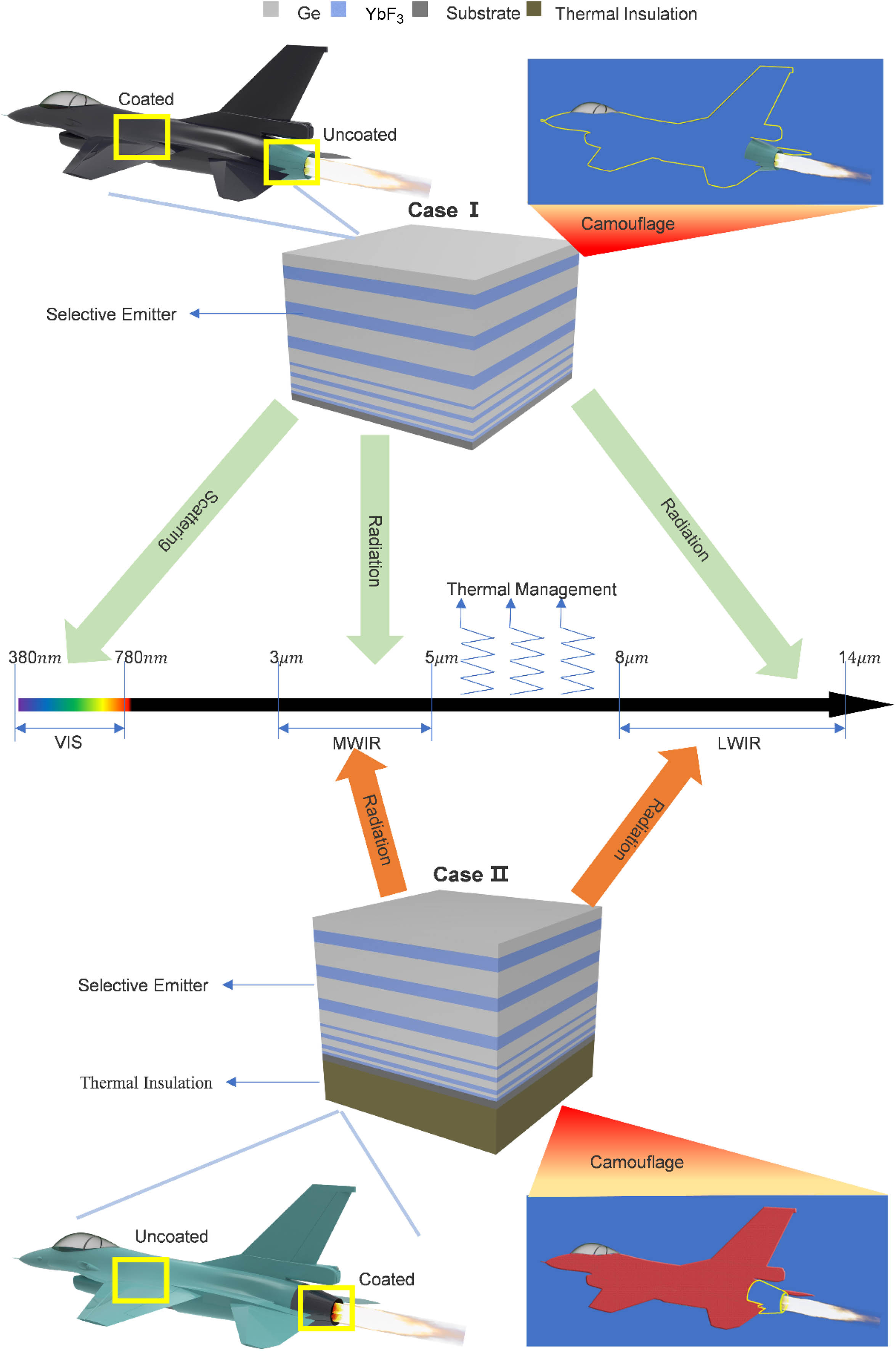
Fig. 1. Schematic of simultaneous multiband camouflage and thermal management in aircraft. Case I. Wavelength-selective emitter with multilayer film structure enables multiband camouflage and thermal management of the aircraft skin. Case II. Emitter combined with thermal insulation enables multiband mid-IR camouflage and thermal management of the aircraft converging nozzle.
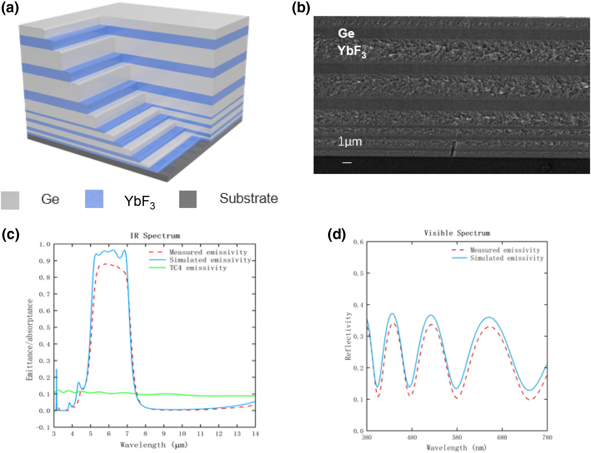
Fig. 2. Simulation and measurements of multilayer film structure. (a) Schematic of the film cladding structure. (b) Scanning electron microscopy image of the prepared Ge / YbF 3
Fig. 3. Schematic of the selective IR emission mechanism of the multilayer film structure. Electric field intensity (E P X Z Y Z
Fig. 4. (a), (b) Emissivity versus wavelength for transverse electric and magnetic polarized waves at oblique incidence angles 0°–40°. (c) For a gradual increase in the incidence angle from 0° to 60°, although the emissivity gradually decreases, the emission band does not deviate from 5–8 μm.
Fig. 5. Diagram of the IR camouflage scheme. (a), (b) Schematic of radiation reflection detection with and without earthshine. (c), (d) Schematic of experimental setup for thermal measurement of radiation cooling performance at background temperatures of 373 and 873 K. (e), (f) Experimental samples at two background temperatures. Samples I and II are directly heated wavelength-selective emitters and titanium alloy references, respectively, and samples III–V are wavelength-selective emitter on aerogel, titanium alloy on aerogel, and bare aerogel, respectively.
Fig. 6. Apparent temperature and thermal IR images (steady state) of different slices. (a), (b) Thermal IR image captured by the detector with a background temperature of 373 K at daytime/nighttime for the 3–5 μm range. The wavelength-selective emitter is sample I and the titanium alloy reference is sample II. (c), (d) Thermal IR image captured by the detector with a background temperature of 373 K at daytime/nighttime for the 8–14 μm range. (e), (f) Thermal IR image captured by the detector with a background temperature of 873 K at daytime/nighttime for the 3–5 μm range. The wavelength-selective emitter is sample III, the titanium alloy reference is sample IV, and the silica aerogel is sample V. (g), (h) Thermal IR image captured by the detector with a background temperature of 873 K at daytime/nighttime for the 8–14 μm range.
Fig. 7. Apparent temperature change with increasing temperature for different samples. (a), (b) Apparent temperature change measured at 373 K background temperature using a 3–5 μm detector at daytime/nighttime. (c), (d) Apparent temperature change measured at 373 K background temperature using a 8–14 μm detector at daytime/nighttime. (e), (f) Apparent temperature change measured at 873 K background temperature using a 3–5 μm detector at daytime/nighttime. (g), (h) Apparent temperature change measured at 873 K background temperature using a 8–14 μm detector at daytime/nighttime.
Fig. 8. Refractive index n k YbF 3
Fig. 9. Emission spectra of multilayers before heating (blue dashed line) and after heating at 623 K for 1 h (orange dashed line).
|
Table 1. Number of Layers and Thickness of Film Obtained from Particle Swarm Optimization

Set citation alerts for the article
Please enter your email address
© Copyright 2018-2021 | Chinese Laser Press. All Rights Reserved 沪ICP备15018463号-20