
Yawen Bai, Pengfei Wang, Bo Peng, Tao Chu. O-band reconfigurable silicon polarization rotator[J]. Chinese Optics Letters, 2024, 22(1): 011303
- Chinese Optics Letters
- Vol. 22, Issue 1, 011303 (2024)
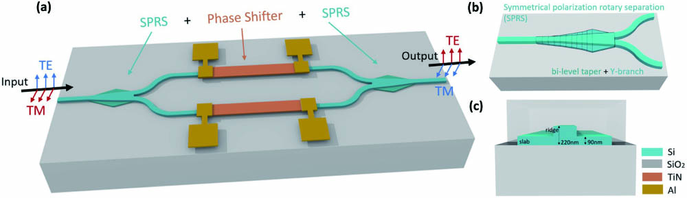
Fig. 1. (a) Overall structure of a rotating device with reconfigurable polarization; (b) structure of the SPRS; (c) side view of the waveguide.
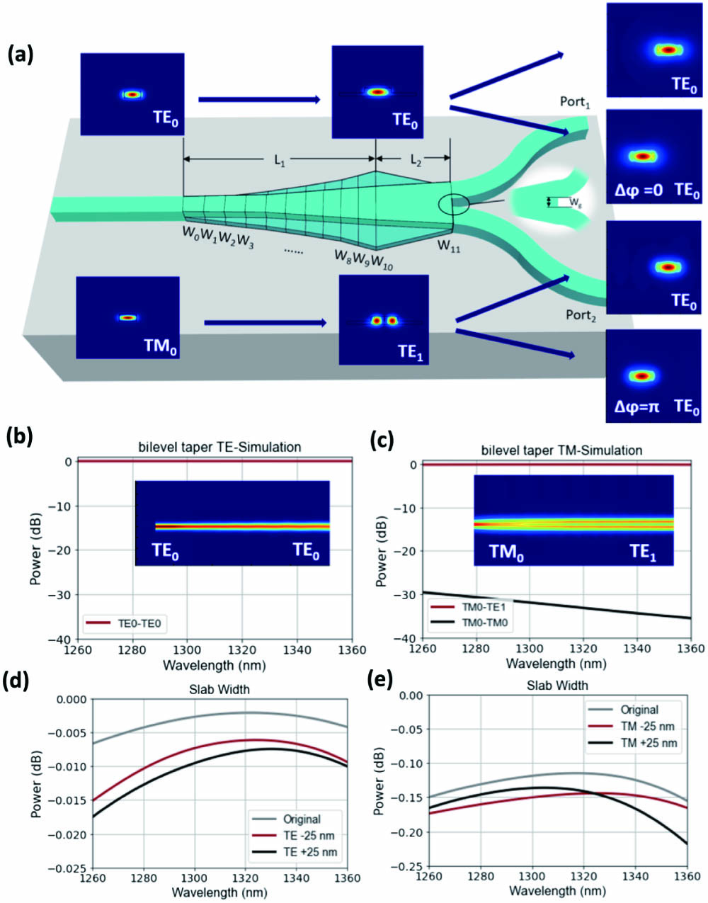
Fig. 2. (a) SPRS structural parameters and working principle; bilevel taper simulations and light-field diagrams of (b) TE and (c) TM; (d) bilevel taper loss at different slab widths (TE); (e) bilevel taper loss at different slab widths (TM).
Fig. 3. (a) SPRS simulation results and light-field diagram (TE); (b) SPRS simulation results and light-field diagram (TM); (c) SPRS loss at different slab thicknesses, and the spectroscopic ratio of port 1 and port 2 (TE); (d) SPRS loss at different slab thicknesses, and the spectroscopic ratio of port 1 and port 2 (TM); (e) reflection scene at Wg; (f) loss of Y-branches at different linewidths of Wg (TE); (g) loss of Y-branches at different linewidths of Wg (TM).
Fig. 4. Microscope scan of the device (a) with TE grating input and TM grating output; (b) with TM grating input and TE grating output; (c) with TE grating input and TE grating output; (d) with TM grating input and TM grating output; reference grating of (e) TE and (f) TM.
Fig. 5. (a) IL of TE–TE and PER of TE–TM; (b) IL of TM–TM and PER of TM–TE; (c) IL of TE–TM and PER of TE–TE; (d) IL of TM–TE and PER of TM–TM; voltage sweep curve of the devices with the reference gratings of (e) TE–TE; (f) TM–TM; (g) TE–TM; and (h) TM–TE.
|
Table 1. PSO Parameters for Bilevel Taper Devices
|
Table 2. Comparison of the Silicon-Based O-band Polarization-Treating Devices

Set citation alerts for the article
Please enter your email address
© Copyright 2018-2021 | Chinese Laser Press. All Rights Reserved 沪ICP备15018463号-20