
Yawen Bai, Pengfei Wang, Bo Peng, Tao Chu. O-band reconfigurable silicon polarization rotator[J]. Chinese Optics Letters, 2024, 22(1): 011303
- Chinese Optics Letters
- Vol. 22, Issue 1, 011303 (2024)
Abstract
1. Introduction
Silicon-based optoelectronic integration is considered one of the most promising technologies for achieving high-density integrated photonic devices owing to its compact structure, low cost, and compatibility with CMOS manufacturing processes[1]. However, the inherent asymmetry of silicon waveguides results in a significant refractive-index difference between the TE and TM modes, leading to substantial polarization correlation in silicon photonic devices[2]. To address this challenge, various polarization-independent and polarization–diverse solutions have been proposed, including polarization beam splitters (PBSs), polarization rotators (PRs), and polarization separation rotators (PSRs)[3–6]. These devices depend on disrupting the symmetry between the horizontal and vertical directions of the waveguide through structures such as dual-core waveguides, asymmetric directional couplers (ADCs), bilevel tapers, metasurface waveguides, bend waveguides, and adiabatic couplers[7–10].
However, existing solutions are predominantly static and fixed, permitting only nonadjustable polarization-control operations. For applications such as coherent communication[11], quantum computing[12], advanced modulation[13], and polarization diversity[14], reconfigurable polarization rotators, including polarization switches and dynamic polarization modulators, offer the advantage of dynamically adjusting the ratio of two polarization states. Unfortunately, there are a limited number of tunable polarization-control devices based on silicon waveguides. According to our research, most of the existing reconfigurable polarization-control devices primarily operate in the C-band[15–19]. The C-band is more commonly used for coherent communication due to its lower loss. With its low dispersion, the O-band is predominantly utilized in data centers, optical module applications, and polarization-encoded quantum technologies[20–23], where dynamically tunable polarization-control devices are essential. There is an urgent need to develop low-loss, high extinction ratio, and compact reconfigurable polarization rotators operating in the O-band.
In this work, we first demonstrate a reconfigurable O-band polarization rotator. The device architecture is further simplified by introducing symmetrical polarization rotator splitters (SPRSs). The SPRS is composed of a bilevel taper and a Y-branch. The incorporation of this feature allows for a reduction in the device’s dimensions while simultaneously enhancing its bandwidth. Compared to the C-band, the O-band’s shorter operating wavelengths require stricter linewidth tolerances and are more sensitive to manufacturing errors. We use particle swarm optimization (PSO) to optimize the device for better performance. According to the experimental results, the insertion loss (IL) values for TE–TE, TM–TM, TE–TM, and TM–TE were 1.44, 0.71, 1.48, and 1.34 dB, respectively, whereas the polarization extinction ratio (PER) values for TE–TM, TM–TE, TE–TE, and TM–TM were 18, 15, 22, and 20 dB, respectively. Compared to previously reported tunable polarization rotators, the device exhibits good IL and PER performance, with an operational bandwidth of 60 nm in the O-band and a total device length of 500 µm. Furthermore, the device’s linewidth is compatible with a 130-nm CMOS silicon-on-insulator (SOI) process and exhibits good process tolerance, offering the potential for large-scale manufacturing.
Sign up for Chinese Optics Letters TOC. Get the latest issue of Chinese Optics Letters delivered right to you!Sign up now
2. Design and Simulation
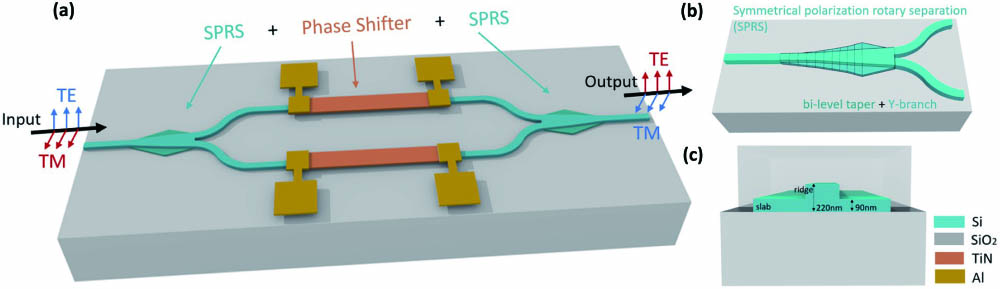
As illustrated in Fig. 1(a), the proposed tunable polarization rotator comprises an SPRS, a phase shifter, and a second SPRS. The device design is based on SOI substrates with a ridge-waveguide height of 220 nm and a slab height of 90 nm, incorporating cladding layers above and below. The device operates such that when no voltage is applied to the phase shifter, the input and output polarizations remain constant. Conversely, when a voltage is applied across the phase shifter, generating a phase difference between the arms, the polarization of the input and output transitions to quadrature, allowing for arbitrary switching between the and polarization states by controlling the phase-shifter voltage.
![]()
Figure 1.(a) Overall structure of a rotating device with reconfigurable polarization; (b) structure of the SPRS; (c) side view of the waveguide.
SPRSs are specialized PSRs. When entering TE, the two output ports exhibit equal phase and amplitude in the TE state; however, when entering TM, the two output ports display equal amplitude and opposite phases in the TE state. The incorporation of SPRS necessitates only a conventional phase shifter to achieve 0−π phase adjustment of TE light, thereby reducing the length of the phase shifter to 100 µm from approximately 700 µm[24]. The application of the SPRS streamlines the device and significantly reduces its size, effectively enhancing its bandwidth.
The mode conversion process and the corresponding Jones matrix are represented in Eq. (1),
In this equation, is a parameter related to the SPRS design structure, and represents the phase difference between the phase shifters. In this study, we utilized a bilevel taper and a Y-branch to implement the SPRS function.
The function of the bilevel taper is to complete the mode conversion of while keeping constant, thereby achieving a compact design that minimizes the device area. When the waveguide structure possesses horizontal and vertical symmetry, no coupling occurs between the TE and TM polarizations. However, when this symmetry is disrupted, coupling may transpire between the and higher-order TE modes. A ridge waveguide, depicted in Fig. 2(a), was employed to break this symmetry. This structure has been extensively studied[25], and our design utilizes PSO algorithms to optimize the device. The specific process entails selecting the device length, which is set to 20 µm and divided into 10 segments. The width of the input single-mode waveguide () is set to 400 nm, the output dual-mode waveguide width () is set to 800 nm, the slab width () is set to 1600 nm, and the waveguide height is set to 90 nm. L2 is set to 30 µm to decrease the device loss. The average conversion efficiency of in the O-band serves as the figure of merit (FOM),
![]()
Figure 2.(a) SPRS structural parameters and working principle; bilevel taper simulations and light-field diagrams of (b) TE and (c) TM; (d) bilevel taper loss at different slab widths (TE); (e) bilevel taper loss at different slab widths (TM).
Subsequently, the PSO algorithm was employed to iteratively optimize the device until an optimal solution was attained. The device parameters determined by the PSO algorithm are presented in Table 1. A three-dimensional finite-difference time-domain (FDTD) simulation was then performed to evaluate device performance. Figures 2(b) and 2(c) depict the simulation results of the bilevel taper: within the 1260–1360-nm wavelength range, the conversion efficiency between and modes exceeded 97.4%, whereas the mode cross talk remained below 30 dB, and the IL of the mode was less than 0.02 dB. Concurrently, an analysis was conducted on the process error of the bilevel taper width, as illustrated in Figs. 2(d) and 2(e). Simulation results indicated that, with a slab width variation of , the transmission loss of remained below 0.02 dB, and the conversion efficiency of stayed above 96.6%, with a loss of less than 0.23 dB. These findings substantiate the relative insensitivity of the bilevel taper width to process error.
| W0 | W1 | W2 | W3 | W4 | W5 | W6 | W7 | W8 | W9 | W10 | |
|---|---|---|---|---|---|---|---|---|---|---|---|
| Ridge (nm) | 400 | 439 | 475 | 509 | 540 | 570 | 598 | 625 | 651 | 676 | 700 |
| Slab (nm) | 400 | 738 | 963 | 1145 | 1302 | 1442 | 1570 | 1688 | 1798 | 1902 | 2000 |
Table 1. PSO Parameters for Bilevel Taper Devices
The dual-mode Y-branch structure facilitates mode conversion, enabling the division of an input wave into two beams with a phase difference, or the division of an input wave into two beams with equal phases. This process simultaneously accomplishes power-equal division and beam combination functions. Given that the thermo-optic coefficient of silicon (Si) is , significant thermo-optic effects can be achieved. Consequently, a 100-µm-long titanium nitride (TiN) is employed as a thermal phase shifter to control the phase by modulating the voltage. Upon adjusting the phase using the phase shifter, two beams with a phase difference are combined to generate light, which is ultimately output in the state. In contrast, two beams with identical phases are combined to produce light. Owing to process variations, the linewidth () of the Y-branch had to be adjusted. The FDTD method was utilized to simulate the SPRS phenomenon. As depicted in Figs. 3(a) and 3(b), when the linewidth () is equal to 140 nm, the losses amount to 0.54 dB for the input mode and 0.29 dB for the input mode. We also analyzed the reflection scene at ; Fig. 3(e) shows that the reflection of is less than 16 dB, and the reflection of is less than 30 dB, which can be ignored. Owing to process variations, both the width and the slab thickness frequently deviate, necessitating a process tolerance analysis. Figures 3(c) and 3(d) show the loss of SPRS at different etching depths under a 1310-nm wavelength when is set to 140 nm, revealing that the TE/TM losses remain below 0.6 dB and the power ratio between ports 1 and 2 remains close to 1 within a thickness range of 50 to 120 nm. This demonstrates the insensitivity of the etched depth. Figures 3(f) and 3(g) illustrate the impact of width on the Y-branch loss at a 1310-nm wavelength when the slab thickness is 90 nm, indicating that the TE loss remains below 0.7 dB. Further, the TM loss is less than 0.2 dB when varies within 0 to 160 nm. These results validate the robust process tolerance of the device.
![]()
Figure 3.(a) SPRS simulation results and light-field diagram (TE); (b) SPRS simulation results and light-field diagram (TM); (c) SPRS loss at different slab thicknesses, and the spectroscopic ratio of port 1 and port 2 (TE); (d) SPRS loss at different slab thicknesses, and the spectroscopic ratio of port 1 and port 2 (TM); (e) reflection scene at Wg; (f) loss of Y-branches at different linewidths of Wg (TE); (g) loss of Y-branches at different linewidths of Wg (TM).
3. Fabrication and Test Results
We fabricated the device at Advanced Micro Foundry Pte Ltd. (AMF) and assessed its performance to confirm its compatibility with CMOS integration. As illustrated in Fig. 4, we utilized a polarization-control analyzer and a three-paddle fiber polarization controller to ensure consistent input and output polarization states. Moreover, TE and TM gratings were employed to couple the light into the chip while monitoring variations in polarization states corresponding to different output responses. These gratings were uniformly etched at 70 nm. The microscope picture and test results of the reference gratings of TE and TM are shown in Figs. 4(e) and 4(f).
![]()
Figure 4.Microscope scan of the device (a) with TE grating input and TM grating output; (b) with TM grating input and TE grating output; (c) with TE grating input and TE grating output; (d) with TM grating input and TM grating output; reference grating of (e) TE and (f) TM.
Initially, the reference grating was tested independently. After calibrating the input polarization state, we conducted IL tests on TE–TE and TM–TM devices without phase shift, maintaining constant polarization states for the input and output emissions, as demonstrated in Figs. 5(a) and 5(b). Within the 1280–1340-nm wavelength range, the losses for TE–TE and TM–TM were measured at 1.44 and 0.71 dB, respectively. To evaluate the performance of TE–TM and TM–TE devices, it was crucial to control the thermal phase shifter via voltage sweeping, with the voltage corresponding to the lowest loss point being indicative of the orthogonal rotation of the polarization state. During the testing process, we initially conduct voltage scanning at the 1310 nm wavelength point. Upon identifying the voltage that prompts an orthogonal rotation of the polarization state, we fix this voltage and proceed with wavelength scanning. Upon testing, the required power for the phase shifter to complete polarization rotation for TE–TM and TM–TE was 18 and 13 mW, respectively. The discrepancy between the two can be attributed to the random phase differences induced between the two arms due to fabrication imperfections. And the power can be further mitigated by optimizing the structure of the phase shifters. After applying the voltage, the IL test in the polarization-selective state could be conducted. The test results depicted in Figs. 5(c) and 5(d) indicate losses of 1.48 dB for TE–TM and 1.34 dB for TM–TE within a 60 nm bandwidth. Compared to the simulation, larger losses are testing errors. Detailed IL is presented in the insets of Figs. 5(a)–5(d). Utilizing gratings for coupling induces refractive index changes and subsequent ripples due to variances in the grating’s waveguide width.
![]()
Figure 5.(a) IL of TE–TE and PER of TE–TM; (b) IL of TM–TM and PER of TM–TE; (c) IL of TE–TM and PER of TE–TE; (d) IL of TM–TE and PER of TM–TM; voltage sweep curve of the devices with the reference gratings of (e) TE–TE; (f) TM–TM; (g) TE–TM; and (h) TM–TE.
These lead to inevitable oscillations and test errors, since the device under test and reference grating are independent, causing data jitter. Furthermore, due to process errors, a TM reference grating exhibits partial resonance peaks at 1320–1340 nm, resulting in severe data jitter within this range.
The PER test involved scanning the voltage and wavelength of each device. Figures 5(e) to 5(h) present the voltage sweep curves of devices with identical and distinct input and output gratings, respectively. These curves show the polarization-state trends of different devices under varying voltage. The transformation of the curve from minimum to maximum loss reflects the quadrature polarization rotation of the device. The polarization extinction ratio is the voltage difference between the maximum and minimum loss values. The test results revealed that the PER values for TE–TM, TM–TE, TE–TE, and TM–TM devices were 18, 15, 22, and 20 dB, respectively. Within the 1280–1340-nm wavelength range, the PER of CMOS-fabricated devices exceeded 15 dB. In subsequent fabrication processes, end-face coupling can be employed to mitigate the impact of grating coupling on the device’s PER.
To more clearly contrast the performance of our work, Table 2 provides a comparison of silicon-based O-band polarization-treating devices. It can be observed that our device’s IL and PER performance are on par with passive polarization-control devices and are compatible with commercial 130-nm CMOS SOI processes. Furthermore, it offers unique contributions and potential advantages in the field of tunable O-band polarization-control devices.
| Reference | Type | IL (dB) | PER (dB) | Bandwidth (nm) | Linewidth (nm) | Reconfigurable |
|---|---|---|---|---|---|---|
| [ | PSR | 3 | 14 | 1260-1360 | 200 | No |
| [ | PSR | 1 | 20 | 1260–1310 | 140 | No |
| [ | PBS | 2.22 | 10 | 1280–1360; 1510–1590 | 100 | No |
| [ | PBS | 0.8 | 10.9 | 1260–1360; 1480–1640 | 100 | No |
| This work | PR | 1.5 | 15 | 1280–1340 | 140 | Yes |
Table 2. Comparison of the Silicon-Based O-band Polarization-Treating Devices
4. Conclusion
This paper presents the design and simulation of an SOI-based reconfigurable O-band polarization rotation device for polarization switching. The device comprises two SPRSs and a thermally controlled phase shifter. Each SPRS component consists of a bilevel taper and a Y-branch structure, which effectively reduces system complexity and enables arbitrary switching between TE and TM polarization states. Following experimental validation, the IL values of TE–TE, TM–TM, TE–TM, and TM–TE within the 1280–1340-nm wavelength range were measured to be 1.44, 0.71, 1.48, and 1.34 dB, respectively. The PER of the device exceeded 15 dB and had a footprint of . Additionally, the linewidth of this design conforms to CMOS specifications, rendering it suitable for mass production and potential application in silicon-based optoelectronic large-scale integrated chips.
References
[1] A. Rickman. The commercialization of silicon photonics. Nat. Photonics, 8, 579(2014).
[11] X. S. Yao, X. Ma, T. Feng. Fast optical frequency detection techniques for coherent distributed sensing and communication systems. Optical Fiber Communications Conference and Exhibition (OFC), 1(2022).
[21] H. K. Tsang, Y. Tong. Silicon photonics for spatially multiplexed high capacity optical fiber communications. Conference on Lasers and Electro-Optics/Pacific Rim, C11H_1(2020).
[23] J. Zhang, M. Zhu, B. Hua et al. 6G oriented 100 GbE real-time demonstration of fiber-THz-fiber seamless communication enabled by photonics. Optical Fiber Communications Conference and Exhibition (OFC), 1(2022).

Set citation alerts for the article
Please enter your email address
© Copyright 2018-2021 | Chinese Laser Press. All Rights Reserved 沪ICP备15018463号-20