Hairui Gao, Jikang Li, Zhenwu Zhang, Keying Zheng, Honghao Xiang, Qingsong Wei. Research Status and Prospect of Multi-Field Modulated Metal Laser Additive Manufacturing(Invited)[J]. Chinese Journal of Lasers, 2024, 51(10): 1002306
Search by keywords or author
- Chinese Journal of Lasers
- Vol. 51, Issue 10, 1002306 (2024)
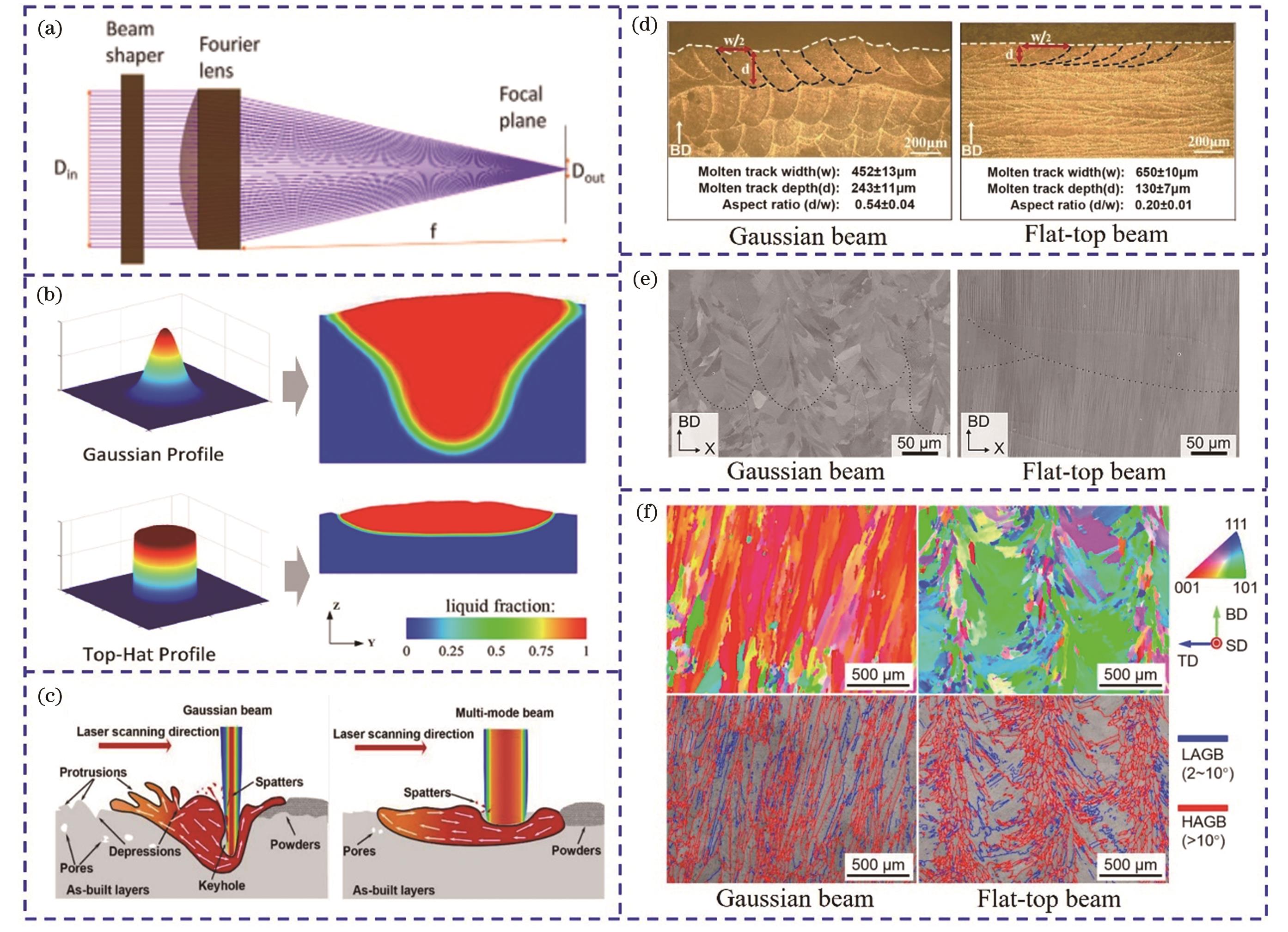
![Comparison of Gaussian and flat-top laser additive manufacturing technology. (a) Schematic diagram of beam shaping[58]; (b) energy distribution and temperature field of melt pool[59-60]; (c) schematic diagram of interaction with powder[68]; (d) OM diagram of AlSi10Mg alloy[68]; (e) SEM image of Ti-Nb alloy[70]; (f) EBSD image of IN718 alloy[76]](/richHtml/zgjg/2024/51/10/1002306/img_01.jpg)
Fig. 1. Comparison of Gaussian and flat-top laser additive manufacturing technology. (a) Schematic diagram of beam shaping[58]; (b) energy distribution and temperature field of melt pool[59-60]; (c) schematic diagram of interaction with powder[68]; (d) OM diagram of AlSi10Mg alloy[68]; (e) SEM image of Ti-Nb alloy[70]; (f) EBSD image of IN718 alloy[76]
![Comparison of Gaussian and anti-Gaussian laser additive manufacturing technology. (a) Shaping principle and two-dimensional energy distribution diagram[78]; (b) SEM image of IN738LC alloy[78]; (c) three-dimensional energy distribution diagram, temperature distribution of melt pool and single-track morphology[80]](/richHtml/zgjg/2024/51/10/1002306/img_02.jpg)
Fig. 2. Comparison of Gaussian and anti-Gaussian laser additive manufacturing technology. (a) Shaping principle and two-dimensional energy distribution diagram[78]; (b) SEM image of IN738LC alloy[78]; (c) three-dimensional energy distribution diagram, temperature distribution of melt pool and single-track morphology[80]
Fig. 3. Comparison of Gaussian and Bessel laser additive manufacturing technology. (a) Schematic diagram of beam shaping, energy distribution and depth-to-width ratio of melt pool; (b) morphology of formed melt pool; (c) EBSD image of prepared 316L alloy[84]
Fig. 4. Comparison of Gaussian and elliptical laser additive manufacturing technology. (a) Spot energy distribution diagram[85]; (b) thermodynamic simulation of melt track X-Y, X-Z and Y-Z plane observations (modes with principal axis of elliptical beam parallel and perpendicular to scanning direction are denoted by LE and TE, respectively)[85,87]; (c) SEM image at melt pool bottom of 316L alloy[85]; (d) EBSD image of side of 316L alloy[86]
Fig. 5. Comparison of additive manufacturing technology between focusing laser and defocusing laser. (a) Schematic diagram of defocusing laser[88]; (b) OM diagrams of IN718 alloy with defocus of 0, 5, 10, 15 and 20 mm, respectively[88]; (c) OM diagram of AlSi10Mg alloy [91]; (d) SEM and EBSD images of side of IN718 alloy[92]
Fig. 6. Substrate preheating assisted laser additive manufacturing technology. (a) OM diagrams of TiAl alloy preheating at 600, 800, 900 ℃[97]; (b) 316L microstructure without preheating and with preheating at 150 ℃[101]; (c) temperature distribution of FeCoMo alloy fabricated at 500 ℃ preheating[106]; (d) EBSD images of TiAl alloy at preheating temperature of 25, 150, 250, 350 ℃[112]; (e) loading-unloading curves and nano-hardness values of TiAl alloy at different preheating temperatures[112]
Fig. 7. Electromagnetic induction heating assisted laser additive manufacturing technology. (a) Comparison of schematic diagram of laser scanning preheating, resistance wire preheating and electromagnetic induction heating[114]; (b) photos of electromagnetic induction heating process and microstructure of TiAl alloy without preheating and with preheating at 800 ℃[114]; (c) schematic diagram of electromagnetic induction-assisted LDED[115]
Fig. 8. Laser scanning preheating assisted laser additive manufacturing technology. (a) Laser synchronous preheating in LDED process[121]; (b) microstructure of 60%IN625-40%Ti6Al4V composites with and without preheating[120]; (c) photos of prepared samples with and without preheating[119]; (d) diagram of laser scanning assisted SLM process[123]
Fig. 9. Static magnetic field assisted laser additive manufacturing technology. (a) Schematic diagram of static magnetic field-assisted SLM and field intensity distribution[133]; (b) 3D simulation results of thermal electromagnetic force acting on dendrites in 0.12 T static magnetic field[133]; (c) EBSD image of AlSi10Mg alloy prepared by SLM with 0.85 mT and without static magnetic field[130]; (d) schematic diagram of thermal electromagnetic force-induced dendrite breakage[17]; (e) tensile stress-strain curves and mechanical properties of AlSi10Mg prepared by SLM with the assistance of 0, 0.1, 0.2 and 0.3 T magnetic fields[17]
Fig. 10. Alternating magnetic field assisted laser additive manufacturing technology. (a) Schematic diagram of alternating magnetic field-assisted SLM[143]; (b) EBSD image of 316L alloy prepared under 0.4 mT, 300 Hz alternating magnetic field and no magnetic field[143]; (c) solidification behavior of melt pool in synchronous electromagnetic induction-assisted LDED process[144]; (d) micro-morphology of TiC enhanced Ti6Al4V alloy with and without high-frequency electromagnetic field[144]
Fig. 11. Ultrasonic vibration-assisted laser additive manufacturing technology. (a) Solidification behavior of melt pool in ultrasonic assisted LDED[151]; (b) micro-morphology of IN718 prepared by LDED at different ultrasonic frequencies (0, 25, 33, 41 kHz)[153]; (c) EBSD image of 316L alloy prepared by LDED with 20 kHz and without ultrasonic field[154]; (d) OM diagram of 316L stainless steel fabricated by LDED with and without ultrasonic field assistance[156]
Fig. 12. Ultrasonic impact-assisted laser additive manufacturing technology. (a) Scan strategy[159]; (b) microscope images of LDED-fabricated IN100 superalloy with and without 75 N ultrasonic impact[159]; (c) inverse pole figure (IPF) mappings, kernel average misorientation (KAM), and grain boundary (GB) distribution of LDED-fabricated IN718 with and without ultrasonic impact[165]

Set citation alerts for the article
Please enter your email address


