
Sanghoon Lee, Sunjae Chung, Hakjoon Lee, Xinyu Liu, M. Dobrowolska, J. K. Furdyna. Interlayer exchange coupling in (Ga,Mn)As ferromagnetic semiconductor multilayer systems[J]. Journal of Semiconductors, 2019, 40(8): 081503
- Journal of Semiconductors
- Vol. 40, Issue 8, 081503 (2019)
Abstract
1. Introduction
Interlayer exchange coupling (IEC) in magnetic multilayers is a spin interaction that determines spontaneous alignment of magnetization between magnetic layers. The magnetization alignment, either parallel or anti-parallel, between two adjacent ferromagnetic layers causes different scattering of charge carriers. The magnitude of electric current passing through a magnetic multilayer structure is then modulated by the relative orientation of magnetization vectors between ferromagnetic layers reaching its maximum for parallel and minimum for antiparallel configuration. Such dependence of resistance on the spin configurations in turn leads to the phenomenon known as giant magnetoresistance (GMR), that was first observed in the Fe/Cr/Fe trilayer[
The properties of IEC in metallic ferromagnetic (FM) multilayers have already been extensively investigated in this context, and the ability to control the IEC by structural parameters to be either FM or antiferromagnetic (AFM) is now well established[
A magnetic multilayer based on (Ga,Mn)As ferromagnetic semiconductor is an interesting material system, since the magnetic properties of the (Ga,Mn)As can be controlled by numerous external means, such as gate voltage, magnetic field, strain, and light illumination[
In this paper, we review the IEC phenomena of (Ga,Mn)As-based multilayers investigated by magneto-transport experiments. We have concentrated on describing the spontaneous realization of both antiferromagnetic (AFM) and ferromagnetic (FM) spin alignment between ferromagnetic (Ga,Mn)As layers, which in turn strongly depends on the structural parameters such as non-magnetic spacer thickness and carrier density in the systems. We have also noticed that the IEC in the (Ga,Mn)As-based multilayers is a long-range interaction reaching tens of nanometers. The IEC in the (Ga,Mn)As multilayers can reach the next nearest neighbor (NNN) interaction, which significantly affects magnetization reversal of the systems by showing multi-step transitions correspond to various spin configurations of the structures.
2. Experiment
All (Ga,Mn)As-based multilayer samples were grown by molecular beam epitaxy (MBE) on (001) GaAs substrates. Several series of (Ga,Mn)As-based multilayer structures were designed by varying structural parameters of the multilayers, such as non-magnetic spacer thickness, carrier density, Mn concentration in the (Ga,Mn)As layer, and number of repetitions of the multilayer structures. These sets of samples are referred to as series A through E. Detailed descriptions of the sample structures are given in Table 1[
For the transport measurements, a Hall device with the long dimension along the [110] (or [1-10]) direction was patterned on the specimen by photolithography and dry (or chemical) etching. The Hall device has six probes and the width of the current channel ranges from 10–300μm depending on the sample. Magnetotransport measurements were carried out in a closed cycle cryostat using a cold finger whose temperature can be varied from 3 to 300 K. The PHR measurements were performed using a sample holder designed so as to allow a magnetic field to be applied in arbitrary directions in the plane of the sample. The temperature dependence of resistance in the absence of magnetic field shows resistance peaks, which provides an estimation of Curie temperatures for the (Ga,Mn)As layers[
3. Magnetotransport of the (Ga,Mn)As-based multilayers
3.1. Observation of FM and AFM interlayer exchange coupling
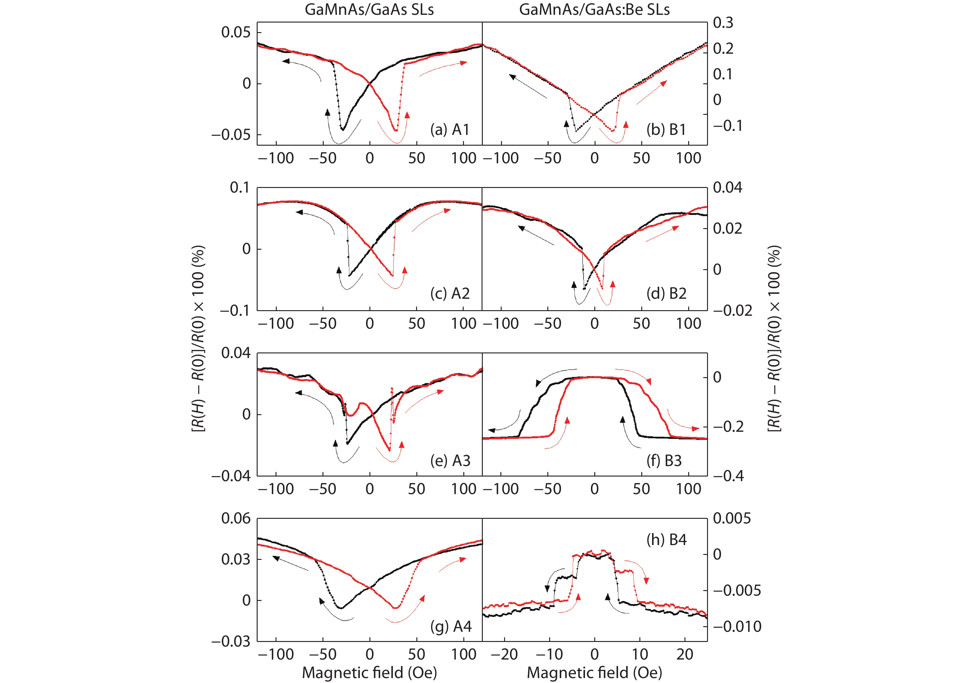
In order to investigate the IEC between (Ga,Mn)As layers, we used magnetoresistance (MR) measurements, which show different values depending on the alignment of magnetization between magnetic layers. We first studied the sample series A and B, which are [(Ga,Mn)As/GaAs]10 and [(Ga,Mn)As/GaAs:Be]10 structure (i.e., the two series are nearly the same except Be in the GaAs spacer). The thickness of the non-magnetic GaAs spacer was systematically varied from 0.7–7.1 nm within each series. These two series of samples were designed to address the dependence of IEC on the spacer thickness and on the carrier density of the (Ga,Mn)As multilayers. Measurements were performed at 30 K with current along the [1-10] direction (i.e., long dimension of the Hall device for sample series A and B) and the external field applied near the [110] crystallographic direction. The temperature of 30 K was selected in order to maximize IEC effect during the magnetization reversal process, which was dominated by crystalline anisotropy at low temperature[
![]()
Figure 1.(Color online) Magnetoresistance of (Ga,Mn)As/GaAs multilayers measured with magnetic field applied near the [110] direction at
In contrast, the MR data obtained from series B shows quite different behavior during the magnetization reversal process. While the B1 and B2 samples with thin GaAs:Be spacer (i.e, 1.2 and 2.3 nm) show typical AMR of a single layer (Ga,Mn)As film (see top two panels in the right column of Fig. 1), other two samples (B3 and B4) clearly show that the lowest resistance occurs at saturated states with large field, and the highest resistance occurs at zero field. Since the parallel and antiparallel alignments give small and large resistance, respectively, in the magnetic multilayer, the magnetization of (Ga,Mn)As layers are parallel in large fields and antiparallel at zero field. Such spontaneous alignment of antiparallel configuration between (Ga,Mn)As layers at zero field clearly indicates the presence of AFM IEC in these two samples. Specially, as the field strength is reduced in returning sweep, the resistance value returns to maximum even before the field direction is reversed. This is because the magnetization alignment between successive (Ga,Mn)As magnetic layers is recovered to antiparallel by AFM IEC with reducing field strength. The investigation of series A and B reveals that the presence of carrier in the GaAs spacer layer is critical for the realization of AFM IEC between (Ga,Mn)As layers and types of IEC can be changed between FM and AFM by varying spacer thickness.
The IEC investigation was further extended to diverse multilayer structures with different structural parameters listed as series C–E in Table 1. In those series, however, the non-magnetic spacer layer was always doped with Be to increase the possibility of observing AFM IEC, which was shown only in Be doped samples in the results of series A and B as described above. For these samples, the Hall device was patterned with long direction (i.e, current direction) along the [110] direction. The MR measurements were performed with the external field along the [110] crystallographic direction. The MR data taken from six representative samples (two samples from each series C, D, and E) are plotted inFig. 2, where the panels in the first and the second rows show data obtained at 3 and 30 K, respectively. All the data in the first row shows typical AMR behavior of single layers of (Ga,Mn)As grown on GaAs substrates as already discussed above. This is because magnetic anisotropy of (Ga,Mn)As layer at low temperature is very strong and it dominates the magnetization reversal process. In contrast, when temperature increases to 30 K, the magnetic anisotropy of (Ga,Mn)As layer significantly decreases[
![]()
Figure 2.(Color online) Magnetoreistance observed in six (Ga,Mn)As/GaAs multilayers with different structural parameters. Samples C1, D1, and E2 show only anisotropic magnetoresistance (AMR), characteristic of FM IEC between the (Ga,Mn)As layers; Samples C3, D2, and E3 show a GMR-like behavior, indicating the presence of AFM IEC in these samples similar to that seen in the [(Ga,Mn)As/GaAs:Be]10 multilayer discussed in detail in the
In order to see the dependence of the IEC on the structure parameters, we have generated plots summarizing the results of all samples. Fig. 3 shows the plot of non-magnetic spacer thickness (vertical axis) versus carrier concentration (horizontal axis) for the multilayer sample. The open red circles and open black squares correspond to the samples showing AFM and FM IEC, respectively. Note that the two symbols are positioned in two isolated regions marked with red and blue backgrounds in Fig. 3. The red circles representing the samples with AFM IEC appear only in the isolated region bounded by the carrier concentration of 1.00 × 1020 cm−3 and by the spacer thickness of 3.5 nm. However, the samples showing FM IEC (i.e., presented with black squares) spread out over a wide range of spacer thickness when the carrier concentration is below 1.25 × 1020 cm−3. This behavior indicates that the carrier concentration as well as spacer thickness are crucial parameters for the realization of AFM IEC in (Ga,Mn)As multilayers.
![]()
Figure 3.(Color online) Summary plot of IEC type for the various (Ga,Mn)As multilayers depending on carrier concentrations and spacer layer thicknesses. Black open squares and red open circles show FM IEC and AFM IEC, respectively. (Adapted from Ref. [
Note further that the spacers in our AFM IEC samples are as thick as 7 nm (i.e., sample B4), which is much greater than those typically used for ferromagnetic metal-based multilayer systems[
3.2. Observation next-nearest-neighbor (NNN) IEC between (Ga,Mn)As layers
Magnetization reversal of magnetic multilayers, in which magnetic layers are coupled to each other, can be strongly affected by exchange coupling. Even though the nature of IEC has been intensively studied in systems involving various ferromagnetic (FM) materials[
The (Ga,Mn)As-based multilayers has special implications in investigating the effects arising from higher-order IEC due to the long-range nature of IEC as mentioned in the previous section. The IEC can reach other (Ga,Mn)As layers over the NN in multilayer structures consisting of more than two magnetic layers. The magnetization reversal process of such multilayers will be significantly modified and will be more complicated by the influence of NNN IEC. Here, we focus on the sample B4 (i.e., [(Ga,Mn)As/GaAs:Be]10 structure that was shown in the third panel of the second column in Fig. 1) in order to show the effect of NNN IEC in the magnetization reversal of (Ga,Mn)As-based multilayers.
Fig. 4(a) shows MR data obtained during magnetization reversal with the applied magnetic field oriented near the [110] direction at 35 K. The data show many transition steps in the saturation (i.e, increasing the field in either direction, which eventually aligns the magnetization of all (Ga,Mn)As layers parallel) and the restoring sweeps (i.e, reducing the field to zero) marked as S1–S4 and R1–R4, respectively. This implies that the magnetizations of those (Ga,Mn)As layers reverse independently as the field increases or decreases in the reversal process.
![]()
Figure 4.(Color online) The process of magnetization reversal in the [(Ga,Mn)As/GaAs:Be]10 multilayer system. (a) MR is measured at 35 K as the field is cycled between −100 and 100 Oe. The down- and up-scans, shown by solid (blue) and open (red) circles, respectively, have a completely symmetrical behavior. Two types of fully AFM spin configurations between the (Ga,Mn)As layers, AFM1 and AFM2, can be realized at zero field, as shown schematically by the vertical arrows. Each field scan (down or up) contains a four-step restoring process and a five- step saturation process, with resistance plateaus marked as R1–R4 and S1–S4. (b) The number of pairs with AFM alignment between adjacent (Ga,Mn)As layers in the multilayer is obtained by minimizing the IEC energy given by Eq. (1) during the down-scan of the field. The field is scaled in terms of the NN IEC strength
In magnetic multilayer system with strong AFM IEC, the magnetic layers form two types of anti-parallel spin configurations, AFM1 (
The interlayer exchange coupling energy E of the our [(Ga,Mn)As/GaAs:Be]10 SL in the presence of a magnetic field H by including NNN IEC contributions can be expressed in the form[
where J1 and J2 are the NN and NNN IEC constants, respectively, and Mi is the magnetization of the ith magnetic layer. The magnetic field dependence of the IEC energy for various spin configurations without NNN IEC contribution in Eq. (1) only explains two step-transitions (i.e., first the outermost magnetic layer and all interior magnetic layers initially aligned opposite to the field) in both the saturation and the restoring processes[
However, when the strength of NNN IEC, J2 = 0.25J1, is included in the calculation, the energy dependences of spin configurations are altered and many possible transitions appear in the restoring and saturation process. The magnetization reversal path obtained by calculating the lowest coupling energy for the down-scan case is shown in Fig. 4(b), which reproduces the observed four-step restoration and the five-step saturation processes. The spin configurations during down-scan are schematically shown in the Fig. 4(b). The detailed calculation and identification of spin configurations correspond to transitions are given in Ref. [40]. Interestingly, R4 and R3 states have the same energy at Hc (see inset of Fig. 4(b)) resulting in the four-step restoration.
Since the transition fields are all different for the (Ga,Mn)As layers in the multilayer system, the magnitude of the total IEC acting on each (Ga,Mn)As layer can be different. The magnitude of the IEC acting on each magnetic layer in [(Ga,Mn)As/GaAs:Be]10 multilayer was investigated by Chung et al.[
3.3. Quantitative determination of NNN IEC between (Ga,Mn)As layers
The multi-step transitions that are observed from (Ga,Mn)As multilayers can be understood based on the sequence of spin alignments between the (Ga,Mn)As layers which is experienced during magnetization reversal. In order to describe this effect theoretically, the strength of NNN IEC was taken to be one quarter of the NN IEC considering the geometry of the multilayer[
![]()
Figure 5.(Color online) Magnetic field dependence of MR and IEC energy during (a) up-scan and (b) down-scan of applied field for samples used in this study. The experimentally measured MR at 23 K and calculated IEC energy for possible spin configurations are plotted in left and right columns of each figure, respectively. (Adapted from Ref. [
The minor hysteresis loop formed by magnetization reversal of only one specific (Ga,Mn)As layer provides the information on the IEC field felt by a given (Ga,Mn)As layer. Fig. 6 shows such minor loops obtained from the negative field region (i.e, minor loop of MR data shown in Fig. 5(a)) for all three structures. The arrows in Fig. 6 show the initial and final spin alignments for each minor loop. As can be seen from the spin configurations, only one (Ga,Mn)As layer experiences magnetization reversal during minor loop scans. The shift of hysteresis, therefore, is proportional to the total IEC strength felt by that specific (Ga,Mn)As layers. The (Ga,Mn)As layer experiencing the magnetization reversal in minor scan has one NN for the structure with 2 (Ga,Mn)As layers and two NN for the structure with 3 (Ga,Mn)As layers. In the case of structure with 5 (Ga,Mn)As layers, it has two NN and two NNN (Ga,Mn)As layers. By considering spin configurations that experienced during the minor scan, the IEC field, HIEC, acting on the (Ga,Mn)As layer can be calculated using Eq. (1). The (Ga,Mn)As layer was counted from the top and we use the magnetization Mi of ith layer for the calculation of the HIEC, which can be related with the NN and NNN IEC coupling constants, J1 and J2, as shown in the Table 2.
![]()
Figure 6.(Color online) Minor MR hysteresis loops obtained during the “restoring” process for our three samples. The minor loops are plotted with red open circles on top of main loops shown by black lines. The magnetization alignments involved in the minor loop of each sample are schematically shown by arrows at corresponding values of MR. The solid vertical lines indicate minor loop shifts HMLS from zero field. (Adapted from Ref. [
The values of HIEC calculated using Eq. (1) for a (Ga,Mn)As layer as it experiences a magnetization reversal are listed in the second column of Table 2. These values can be compared to the experimentally observed minor loop shift HMLS listed in the fourth column. The values are normalized to the 2-layer sample, as listed in the third and fifth columns of Table 2, for direct comparison. The calculation shows that the HIEC is two times larger for the 3-layer structure than for the 2-layer structure. This is because, while the 2-layer (Ga,Mn)As structure has only one (Ga,Mn)As NN, the middle (Ga,Mn)As layer in the 3-layer structure has a (Ga,Mn)As NN layer on both sides, doubling the strength of NN IEC that acts on the center (Ga,Mn)As layer. This relation is directly observed in experiment in the form of a minor loop shift, which is indeed twice as large in the 3-layer structure as it is in the case of the 2-layer structure, as shown in the fifth column of Table 2. This clearly indicates that the strength of the NN IEC in our samples is nearly constant between any two (Ga,Mn)As layer pairs.
By considering the effect of nearest neighbors, one would expect the HMLS ratio 2.0 in multilayer structures. However, we observed the HMLS ratio of 2.46 in 5-layer structure, which is clearly greater than 2.0. The increased value of 0.46, therefore, can be attributed to the contributions from the NNN IEC in the 5-layer system. This value can be expressed as 2(J2/J1) (as shown in the second column for the 5-layer structure in Table 2). The experiments directly provide a measure of the NNN IEC strength in our system as J2 = 0.23J1. This experimentally determined relative strength of NNN IEC to NN IEC, 0.23, is similar to 0.25, the value extracted by considering simply the distance separating the magnetic layers[
4. Summary and Conclusions
We have investigated IEC phenomena in various types of (Ga,Mn)As-based multilayer structures by using magnetotransport measurements. Investigations of sample series A and B, which are different between series by Be doping in GaAs spacer, show both FM and AFM IEC depending on the structural parameters. Interestingly, AFM IEC was observed only in the Be doped samples (i.e, among series B) indicating that the presence of a carrier in the GaAs spacer is crucial for the realization of AFM IEC in the (Ga,Mn)As-based multilayer. In addition, the AFM IEC even appears in the sample with 7 nm GaAs spacer, which is much thicker than that predicted by theoretical calculation, implying that IEC in the (Ga,Mn)As-based system is quite long-ranged. Such long-ranged magnetic IEC in (Ga,Mn)As-based multilayers provided a unique opportunity for investigation of NNN IEC, which has never been reported in metallic multilayer systems. The effect of NNN IEC in (Ga,Mn)As multilayers indeed observed as interesting step-like transitions during magnetization reversal. Each transition corresponds to the flips of magnetization in specific (Ga,Mn)As layers, which feels a different magnitude of IEC owing to the influence of NNN IEC in the system. The relative strength of NNN IEC to the NN IEC in (Ga,Mn)As multilayers was experimentally determined as 0.23, which is close to the value expected from the theory.
Acknowledgments
This research was supported by Basic Science Research Program through the National Research Foundation of Korea (NRF) funded by the Ministry of Education (2018R1D1A1A02042965); by Ministry of Science ICT (2018R1A4A1024157); by a Korea University Future Research Grant; and by the National Science Foundation Grant DMR 1400432.
References
[1] G Binasch, P Grünberg, F Saurenbach et al. Enhanced magnetoresistance in layered magnetic structures with antiferromagnetic interlayer exchange. Phys Rev B, 39, 4828(1989).
[2] M N Baibich, J M Broto, A Fert et al. Giant magnetoresistance of (001)Fe/(001)Cr magnetic superlattices. Phys Rev Lett, 61, 2472(1988).
[3] S S P Parkin, w R F C Farrow, R F Marks et al. Oscillations of interlayer exchange coupling and giant magnetoresistance in (111) oriented permalloy/Au multilayers. Phys Rev Lett, 73, 1190(1994).
[4] P J H Bloemen, H W van Kesteren, H J M Swagten et al. Oscillatory interlayer exchange coupling in Co/Ru multilayers and bilayers. Phys Rev B, 50, 13505(1994).
[5] J A Borchers, J A Dura, J Unguris et al. Observation of antiparallel magnetic order in weakly coupled Co/Cu multilayers. Phys Rev Lett, 82, 2796(1999).
[6] S S P Parkin. Systematic variation of the strength and oscillation period of indirect magnetic exchange coupling through the 3d, 4d, and 5d transition metals. Phys Rev Lett, 67, 3598(1991).
[7] S S P Parkin, N More, K Roche. Oscillations in exchange coupling and magnetoresistance in metallic superlattice structures: Co/Ru, Co/Cr, and Fe/Cr. Phys Rev Lett, 64, 2304(1990).
[8] L Berger. Emission of spin waves by a magnetic multilayer traversed by a current. Phys Rev B, 54, 9353(1996).
[9] I M Miron, K Garello, G Gaudin et al. Perpendicular switching of a single ferromagnetic layer induced by in-plane current injection. Nature, 476, 189(2011).
[10] J C Slonczewski. Current-driven excitations of magnetic multilayers. J Magn Magn Mater, 159, L1(1996).
[11] S Koshihara, A Oiwa, a M Hirasawa et al. Ferromagnetic order induced by photogenerated carriers in magnetic III–V semiconductor heterostructures of (In, Mn)As/GaSb. Phys Rev Lett, 78, 4617(1997).
[12] H Lee, S Choi, S Lee et al. Effect of light illumination on the [100] uniaxial magnetic anisotropy of (Ga,Mn)As film. Solid State Commun, 192, 27(2014).
[13] S Lee, n D Y Shin, S J Chung et al. Tunable quaternary states in ferromagnetic semiconductor (Ga,Mn)As single layer for memory devices. Appl Phys Lett, 90, 152113(2007).
[14] X Liu, Y Sasaki, J K Furdyna. Ferromagnetic resonance in Ga1−
[15] H Ohno, D Chiba, F Matsukura et al. Electric-field control of ferromagnetism. Nature, 408, 944(2000).
[16] H Lee, S Lee, S Choi et al. Interlayer exchange coupling in MBE-grown (Ga,Mn)As-based multilayer systems. J Cryst Growth, 477, 188(2017).
[17] S K Bac, H Lee, S Kee et al. Effects on magnetic properties of (Ga,Mn)As induced by proximity of topological insulator Bi2Se3. J Electron Mater, 47, 4308(2018).
[18] J Chang, S Bhoi, K J Lee et al. Effects of film thickness and annealing on the magnetic properties of (Ga,Mn)AsP ferromagnetic semiconductor. J Cryst Growth, 512, 112(2019).
[19] S U Yuldashev, m K Im, V S Yalishev et al. Effect of additional nonmagnetic acceptor doping on the resistivity peak and the Curie temperature of Ga1−
[20] S Chung, S Lee, J H Chung et al. Giant magnetoresistance and long-range antiferromagnetic interlayer exchange coupling in (Ga,Mn)As/GaAs: Be multilayers. Phys Rev B, 82, 054420(2010).
[21] S Chung, S Lee, T Yoo et al. Determination of interlayer exchange fields acting on individual (Ga,Mn)As layers in (Ga,Mn)As/GaAs multilayers. Jpn J Appl Phys, 54, 033001(2015).
[22] H Lee, S Lee, S Choi et al. Antiferromagnetic interlayer exchange coupling in ferromagnetic (Ga,Mn)As/GaAs: Be multilayers. IEEE Trans Magn, 51, 2400604(2015).
[23] J Leiner, H Lee, T Yoo et al. Observation of antiferromagnetic interlayer exchange coupling in a Ga1−
[24] D V Baxter, D Ruzmetov, J Scherschligt et al. Anisotropic magnetoresistance in Ga1−
[25] K Y Wang, K W Edmonds, R P Campion et al. Anisotropic magnetoresistance and magnetic anisotropy in high-quality (Ga,Mn)As films. Phys Rev B, 72, 085201(2005).
[26] D Y Shin, S J Chung, S Lee et al. Temperature dependence of magnetic anisotropy in ferromagnetic (Ga,Mn)As films: Investigation by the planar Hall effect. Phys Rev B, 76, 035327(2007).
[27] P A Grünberg. Exchange anisotropy, interlayer exchange coupling and GMR in research and application. Sens Actuators A, 91, 153(2001).
[28] A D Giddings, T Jungwirth, B L Gallagher. (Ga,Mn)As based superlattices and the search for antiferromagnetic interlayer coupling. Phys Rev B, 78, 165312(2008).
[29] P Sankowski, P Kacman. Interlayer exchange coupling in (Ga,Mn)As-based superlattices. Phys Rev B, 71, 201303(2005).
[30] K Szałowski, T Balcerzak. Antiferromagnetic interlayer coupling in diluted magnetic thin films with RKKY interaction. Phys Rev B, 79, 214430(2009).
[31] J H Chung, S J Chung, S Lee et al. Carrier-mediated antiferromagnetic interlayer exchange coupling in diluted magnetic semiconductor multilayers Ga1−
[32] J H Chung, J Lin, J K Furdyna et al. Investigation of weak interlayer exchange coupling in (Ga,Mn)As/GaAs superlattices with insulating nonmagnetic spacers. J Appl Phys, 110, 013912(2011).
[33] H Kępa, V K Le, C M Brown et al. Probing hole-induced ferromagnetic exchange in magnetic semiconductors by inelastic neutron scattering. Phys Rev Lett, 91, 087205(2003).
[34] J J Rhyne, J Lin, J K Furdyna et al. Anomalous antiferromagnetic coupling in [ZnTe¦MnTe] superlattices. J Magn Magn Mater, 177–181, 1195(1998).
[35] J Unguris, R J Celotta, D T Pierce. Observation of two different oscillation periods in the exchange coupling of Fe/Cr/Fe(100). Phys Rev Lett, 67, 140(1991).
[36] P Bruno, C Chappert. Oscillatory coupling between ferromagnetic layers separated by a nonmagnetic metal spacer. Phys Rev Lett, 67, 1602(1991).
[37] P Bruno, C Chappert. Ruderman-Kittel theory of oscillatory interlayer exchange coupling. Phys Rev B, 46, 261(1992).
[38] Y Yafet. Ruderman-Kittel-Kasuya-Yosida range function of a one-dimensional free-electron gas. Phys Rev B, 36, 3948(1987).
[39] B Chen, H Xu, C Ma et al. All-oxide-based synthetic antiferromagnets exhibiting layer-resolved magnetization reversal. Science, 357, 191(2017).
[40] S Chung, S Lee, T Yoo et al. The critical role of next-nearest-neighbor interlayer interaction in the magnetic behavior of magnetic/non-magnetic multilayers. New J Phys, 15, 123025(2013).
[41] K F Eid, M B Stone, K C Ku et al. Exchange biasing of the ferromagnetic semiconductor Ga1−
[42] K M Yu, W Walukiewicz, T Wojtowicz et al. Effect of film thickness on the incorporation of Mn interstitials in Ga1−
[43] H Lee, S K Bac, S Lee et al. Experimental determination of next-nearest-neighbor interlayer exchange coupling in ferromagnetic (Ga,Mn)As/GaAs:Be multilayers. Appl Phys Lett, 107, 192403(2015).
[44] J H Han, H W Lee. Interlayer exchange coupling between next nearest neighbor layers. Phys Rev B, 86, 174426(2012).


Set citation alerts for the article
Please enter your email address

© Copyright 2018-2021 | Chinese Laser Press. All Rights Reserved 沪ICP备15018463号-20