
Baohua Zhu, Fangfang Wang, Guixia Wang, Yuzong Gu. Oxygen-containing-defect-induced synergistic nonlinear optical enhancement of graphene/CdS nanohybrids under single pulse laser irradiation[J]. Photonics Research, 2018, 6(12): 1158
- Photonics Research
- Vol. 6, Issue 12, 1158 (2018)
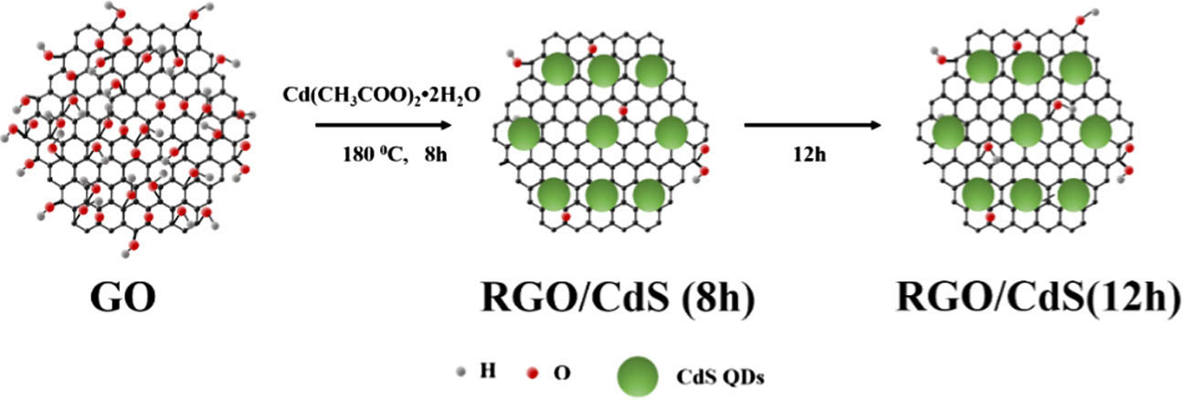
Fig. 1. Schematic illustration of the synthesis procedure of G/CdS NHs.
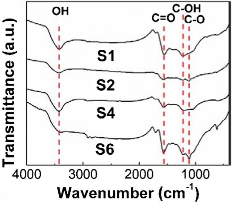
Fig. 2. Typical FTIR spectra of S1, S2, S4, and S6.
Fig. 3. Typical XPS spectra of (a) S1, (b) typical C 1s, and (c) O 1s. (d) Ratio of O and C of the samples.
Fig. 4. TEM images of (a) S1 and (b) S5. HRTEM image of CdS [inset of (a)]. EDX spectra of (c) S2 and (d) S6.
Fig. 5. XRD patterns of the samples.
Fig. 6. (a) Raman spectra and (b) n D
Fig. 7. (a) Absorption spectra of S6 compared with CdS and graphene. (b) Typical absorption spectra of the samples.
Fig. 8. Measured OA Z-scan traces of (a) S6, CdS, and graphene and (b) S3, S4, and S6. (c) The typical β
Fig. 9. Im χ ( 3 ) Re χ ( 3 ) χ ( 3 ) Re χ ( 3 )
Fig. 10. Typical NLO transmission spectrum (S2). The red solid line is the theoretical fitting curve.
Fig. 11. (a) OA Z-scan curves of S6 at 4.2, 5.6, and 6.8 GW / cm 2 4.1 GW / cm 2 5.2 GW / cm 2 T P − V
Fig. 12. PL spectra of S6, GO, and CdS.
Fig. 13. Structural models of G/CdS at different stages of reduction of (a) S2, (c) S4, (e) and S6. The dark gray areas represent sp 2 sp 3

Set citation alerts for the article
Please enter your email address
© Copyright 2018-2021 | Chinese Laser Press. All Rights Reserved 沪ICP备15018463号-20