Abstract
A NiO/β-Ga2O3 heterojunction-gate field effect transistor (HJ-FET) is fabricated and its instability mechanisms are experimentally investigated under different gate stress voltage (VG,s) and stress times (ts). Two different degradation mechanisms of the devices under negative bias stress (NBS) are identified. At low VG,s for a short ts, NiO bulk traps trapping/de-trapping electrons are responsible for decrease/recovery of the leakage current, respectively. At higher VG,s or long ts, the device transfer characteristic curves and threshold voltage (VTH) are almost permanently negatively shifted. This is because the interface dipoles are almost permanently ionized and neutralize the ionized charges in the space charge region (SCR) across the heterojunction interface, resulting in a narrowing SCR. This provides an important theoretical guide to study the reliability of NiO/β-Ga2O3 heterojunction devices in power electronic applications.1. Introduction
β-Ga2O3 has attracted great attention in power electronics because of its ultra-wide bandgap (Eg) of 4.9 eV and high critical electric field of 8 MV/cm. Due to the excellent material properties, the Baliga’s figure of merit (BFOM) is 3444x Si, which is much higher than other wide bandgap materials like SiC and GaN[1, 2]. In recent years, β-Ga2O3 power field-effect transistors (FETs) have achieved tremendous progress in high BFOM[3, 4]. However, the absence of p-type β-Ga2O3 makes the breakdown voltage (BV) and the BFOM far lower than its theoretical limit. To overcome this challenge and obtain the advantages of p-n junction devices, various p-type oxides have been hetero-integrated with β-Ga2O3[5, 6], among which NiO with Eg of 3.8-4 eV and controllable doping concentration is proved to be greatly suitable for β-Ga2O3 power devices[7, 8]. Moreover, great advances have been achieved in BFOM of NiO/β-Ga2O3 power heterojunction FETs[9, 10]. However, the abrupt NiO/β-Ga2O3 heterojunction may produce severe trap effects. These effects include degradation of the threshold voltage (VTH) and current under the negative bias stress (NBS)[11, 12]. Few studies have focused on the critical issue of gate instability in NiO/β-Ga2O3 heterojunction FETs. Therefore, to promote β-Ga2O3 high-power applications in the future, it is important to further our investigation on the degradation mechanism of NiO/β-Ga2O3 heterojunction FETs.
In this work, a NiO/β-Ga2O3 heterojunction-gate FET (HJ-FET) was fabricated and its instability was analyzed at different gate stress voltage (VG,s) and stress times (ts) under negative bias stress (NBS). Two different degradation mechanisms were found: the first is a recoverable degradation owing to NiO bulk traps on the condition of a low VG,s and short ts; and the second is a permanent degradation caused by the ionized interface dipoles in the NiO/β-Ga2O3 heterojunction with large VG,s or ts values.
2. Experimental
2.1. Device fabrication
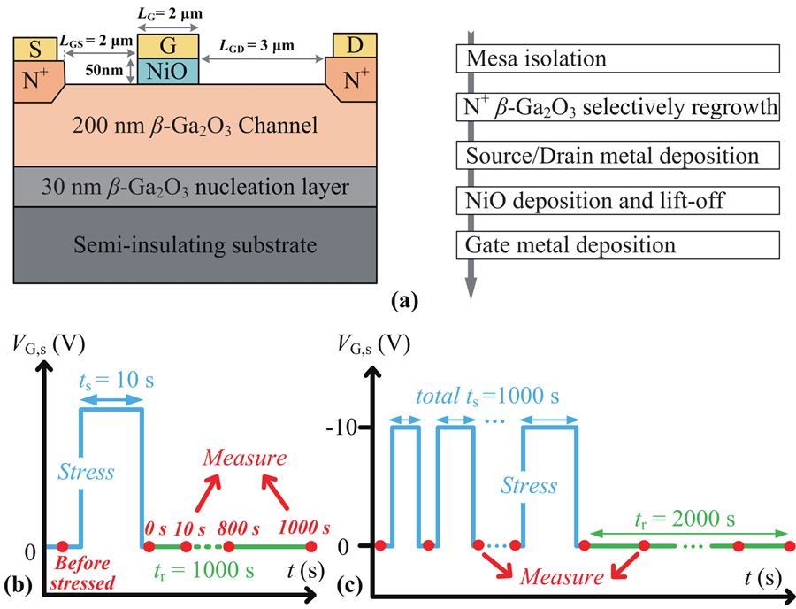
Fig. 1(a) shows the cross-sectional view and process flow of the fabricated NiO/β-Ga2O3 HJ-FET. A 200 nm thick Si-doped β-Ga2O3 epitaxial layer with a concentration of 1 × 1018 cm−3 was grown on the Fe-doped semi-insulating (010) β-Ga2O3 substrate with Agilis R&D MOCVD system. After that, the mesa isolation was realized by an inductively coupled plasma (ICP) process. Using SiO2 as a hard mask, the source and drain N+ regions were selectively regrown by MOCVD with a heavy doping concentration of 1 × 1019 cm−3. Then, to form source/drain ohmic contacts, Ti/Al/Ni/Au (20/160/40/80 nm) were evaporated and followed by rapid thermal annealing (RTA) at 470 °C for 60 s in nitrogen. The p-type NiO was sputtered at room temperature and followed by a lift-off process. The NiO concentration and thickness are 1 × 1019 cm−3 and 50 nm, respectively. Finally, the gate metal Ni/Au (20/80 nm) was fabricated using an e-beam evaporation and lift-off process. The fabricated NiO/β-Ga2O3 HJ-FETs have a gate length (LG) of 2 μm, gate-source separation (LGS) of 2 μm, and gate-drain separation (LGD) of 3 μm.

Figure 1.(Color online) (a) Cross-sectional view of the proposed NiO/β-Ga2O3 HJ-FET and the main fabrication process flows. Schematic representation of the testing method for the analysis instability under NBS at (b) single pulse, and (c) multiple pulses with a prolonged ts.
2.2. Measurement method
The NBS-induced instability of NiO/β-Ga2O3 HJ-FET was experimentally investigated using the Agilent 4155B. The NBS with a constant stress time ts of 10 s experiments were first performed with VG,s = −5 V to −20 V and VDS = 0 V. After the stress was removed, the device enters the recovery process immediately with the gate/source/drain grounded, and the total recovery time (tr) is 1000 s, as shown in Fig. 1(b). Fast measurements are performed during interrupting the recovery processes at pre-set time nodes (from 1 s to 1000 s) to record the I-V characteristics. The NBS with prolonged ts experiments, are characterized by the stress VG,s = −10 V and VDS = 0 V, with the ts from 1 µs to the total ts of 1000 s. After the stress was removed, the device repeats the recovery experiment described above with a total tr of 2000 s, as shown in Fig. 1(c).
3. Results and discussion
Fig. 2(a) represents the transfer characteristic curves of the fabricated NiO/β-Ga2O3 HJ-FET, exhibiting a little hysteresis. Because the electrons in the channel are captured by the interface states in the forward sweeping (−10 V to 0 V), while these captured electrons are not released in time in the backward sweeping (0 V to −10 V). The difference in channel electron density during the forward and backward sweeping causes a little hysteresis. The max IDS ON/OFF ratio of the device is about ~ 109 at VDS = 8 V. The measured output characteristics with specific on-resistance (Ron,sp) are shown in Fig. 2(b). The instability of NBS experiment with a constant ts was first investigated at room temperature. Fig. 3(a) shows the recovery shifts of log-scale transfer characteristic curves after NBS with VG,s = −5 V and ts= 10 s. As shown in Fig. 3(a), the IDS decreases after the stress is just withdrawn, and it almost returns to the value before stressed as the tr increases to 1000 s. The same phenomenon is observed in Fig. 3(b), and the gate current decreases and recovers gradually to its initial after the stress is withdrawn. VTH is extracted from the VGS-IDS curves at IDS = 1 × 10⁻⁵ A and VDS = 8 V[13]. Fig. 3(c) gives the extracted ∆VTH (= VTH − VTH0, VTH0 is the initial VTH without gate bias stress) with a slight positive shift, and VTH almost returns to its initial value after the stress is withdrawn for 1000 s. VG,s = −10 V leads to a larger VTH shift than VG,s = −5 V. The gate off-state current (IGS,off) is defined as the gate current at VGS = −10 V from the VGS-IGS curves. The IGS,off degradation ratio is given as (IGS,off(t) − IGS,off(0))/IGS,off(0). Fig. 3(d) shows that IGS,off decreases by 84% for VG,s = −5 V and then gradually recovers to its initial value. Also, VG,s = −10 V causes a larger decrease in IGS,off of about 87%.
Figure 2.(Color online) Measured DC characteristics: (a) log-scale transfer characteristics and (b) output characteristics.
Figure 3.(Color online) Measured (a) VGS-IDS and (b) VGS-IGS curves after NBS as a function of tr. Extracted (c) ∆VTH and (d) IGS, off degradation ratio.
NiO bulk traps could explain the IGS,off variations. When NBS is applied, electrons injected from the gate are trapped by the acceptor-type bulk traps in NiO, causing the bulk traps to be negatively charged[14]. After the stress is removed, the negatively charged bulk traps block the gate leakage, resulting in a decrease in IGS,off. In terms of transfer characteristics, it will lead to a decrease in IDS and a slight positive shift in VTH. During the recovery phase, these negatively charged bulk traps gradually release the trapped electrons and return to the initial neutral state[15].
The mechanism will change for a high VG,s, as shown in Fig. 4. The NBS experiment in Fig. 4(a) shows an increase in the current of the linear region with the increasing tr at VG,s = −20 V, while the current in the off-region is reduced. The current did not recover significantly in the recovery process nevertheless. The extracted ∆VTH shows that a high VG,s causes a near-permanent negative shift in VTH and a higher VG,s cause a larger shift, as given in Fig. 4(b).
Figure 4.(Color online) Measured (a) VGS-IDS and (b) VGS-IGS curves after NBS as a function of tr. Extracted (c) ∆VTH and (d) IGS, off degradation ratio.
To investigate the instability of NiO/β-Ga2O3 HJ-FET under a prolonged ts, the prolonged ts NBS experiments were performed on another fresh device with the same structure. Fig. 5(a) shows the shifts of log-scale VGS-IDS curves during NBS for different ts. As ts increases, the curves steadily shift negatively, and the saturation current significantly increases. The extracted ∆VTH indicates that the device characteristics are relatively stable at ts < 20 s, but when ts ≥ 20 s, VTH starts to be negatively shifted and eventually decreases by about 2 V, as shown in Fig. 5(b). However, during the recovery process, both the characteristic curves and ∆VTH are not recovered at tr = 2000 s, as shown in Figs. 5(a) and 5(b). This non-recoverable degradation is also illustrated by the equivalent heterojunction diode current VGS-IGS shown in the inset of Fig. 5(b). The VGS-IGS curves shift toward the opposite direction compared to the VGS-IDS curves in Fig. 5(a). As the ts increases, IGS decreases and does not recover at tr = 2000 s. The interface recombination current in the NiO/β-Ga2O3 diode acts as the dominant current transport mode. The decrease in IGS is attributed to a decrease in the recombination centers.
Figure 5.(Color online) (a) Measured VGS-IDS curves during NBS at VG,s = -20 V. (b) Extracted ∆VTH.
Fig. 6 describes the mechanism of the almost permanent degradation under NBS. Due to the energy band discontinuity at the NiO/β-Ga2O3 heterojunction interface, the presence of interface dipoles offsets the internal electric field generated by the ionized impurities in the space charge region (SCR)[16], as shown in Fig. 6(a). These interface dipoles may be considered as charged interface states from two sides of the heterojunction[17]. The larger VG,s generates an extremely large electric field at the interface, which causes some interface dipoles ionize into electrons and holes, as given in Fig. 6(b). Under the stress electric field, electrons and holes move towards β-Ga2O3 and NiO respectively and recombine with the ionized charges in the SCR, resulting in the thinning of the SCR and the decrease in the on-resistance, as shown in Fig. 6(c). This leads to an increase in current and a negative shift in VTH. The almost non-recovery of VTH indicates that this ionization is irreversible. The large potential barrier in the SCR prevents the combined electrons and holes from reorganizing into interface dipoles after the stress is withdrawn. The NiO/β-Ga2O3 heterojunction current (IGS in the inset of Fig. 5(b)) transport is dominated by the interface recombination current[18], and a reduction in interface dipoles lead to the reduction in the recombination centers, which eventually causes the leakage current in the off-region to decrease. We have also shown that interface dipoles are also ionized for prolonged experiments at relatively small VG,s.
Figure 6.(Color online) Schematic cross-sections of NiO/β-Ga2O3 HJ-FET (a) at initial, (b) under NBS, and (c) after NBS, respectively.
4. Conclusion
In summary, the impact of NBS on the electrical characteristics of NiO/β-Ga2O3 HJ-FETs has been studied at different stress voltages and stress times. With low VG,s and ts values, the NiO bulk traps capture electrons to reduce the gate-injected electrons, resulting in a decrease in leakage current. Fortunately, it will fully recover after a long tr. With the increasing stress voltage or stress time, the ionization of the interface dipoles expands the current conduction path leading to an increase in the current and a negative shift in VTH. This is a near-permanent degradation for NiO/β-Ga2O3 heterojunctions and should be considered in engineering.
References
[1] M Higashiwaki, K Sasaki, A Kuramata et al. Gallium oxide (Ga2O3) metal-semiconductor field-effect transistors on single-crystal β-Ga2O3 (010) substrates. Appl Phys Lett, 100, 013504(2012).
[2] W S Li, K Nomoto, Z Y Hu et al. Field-plated Ga2O3 trench Schottky barrier diodes with a BV2/Ron, sp of up to 0.95 GW/cm2. IEEE Electron Device Lett, 41, 107(2020).
[3] Y J Lv, H Y Liu, X Y Zhou et al. Lateral β-Ga2O3 MOSFETs with high power figure of merit of 277 MW/cm2. IEEE Electron Device Lett, 41, 537(2020).
[4] C L Wang, H Zhou, J C Zhang et al. Hysteresis-free and μs-switching of D/E-modes Ga2O3 hetero-junction FETs with the BV2/Ron,sp of 0.74/0.28 GW/cm2. Appl Phys Lett, 120, 112101(2022).
[5] H H Gong, F Zhou, W Z Xu et al. 1.37 kV/12 A NiO/β-Ga2O3 heterojunction diode with nanosecond reverse recovery and rugged surge-current capability. IEEE Trans Power Electron, 36, 12213(2021).
[6] H H Gong, Z P Wang, X X Yu et al. Field-plated NiO/Ga2O3 p-n heterojunction power diodes with high-temperature thermal stability and near unity ideality factors. IEEE J Electron Devices Soc, 9, 1166(2021).
[7] J C Zhang, P F Dong, K Dang et al. Ultra-wide bandgap semiconductor Ga2O3 power diodes. Nat Commun, 13, 3900(2022).
[8] Z P Wang, H H Gong, C X Meng et al. Majority and minority carrier traps in NiO/β-Ga2O3 p-n heterojunction diode. IEEE Trans Electron Devices, 69, 981(2022).
[9] C L Wang, H H Gong, W N Lei et al. Demonstration of the p-NiOx/n-Ga2O3 heterojunction gate FETs and diodes with BV2/Ron, sp figures of merit of 0.39 GW/cm2 and 1.38 GW/cm2. IEEE Electron Device Lett, 42, 485(2021).
[10] X Z Zhou, Q Liu, W B Hao et al. Normally-off β-Ga2O3 power heterojunction field-effect-transistor realized by p-NiO and recessed-gate.. IEEE 34th International Symposium on Power Semiconductor Devices and ICs (ISPSD), 101(2022).
[11] Z L Jiang, J Wei, Y J Lv et al. Nonuniform mechanism for positive and negative bias stress instability in β-Ga2O3 MOSFET. IEEE Trans Electron Devices, 69, 5509(2022).
[12] B Ye, Y Gu, H Xu et al. NBTI mitigation by optimized HKMG thermal processing in a FinFET technology. IEEE Trans Electron Devices, 69, 905(2022).
[13] Z L Jiang, Y X Wei, Y J Lv et al. Experimental investigation on threshold voltage instability for β-Ga2O3 MOSFET under electrical and thermal stress. IEEE Trans Electron Devices, 69, 5048(2022).
[14] A Guo, J A del Alamo. Unified mechanism for positive-and negative-bias temperature instability in GaN MOSFETs. IEEE Trans Electron Devices, 64, 2142(2017).
[15] N Zagni, M Cioni, A Chini et al. Mechanisms underlying the bidirectional VT shift after negative-bias temperature instability stress in carbon-doped fully recessed AlGaN/GaN MIS-HEMTs. IEEE Trans Electron Devices, 68, 2564(2021).
[16] H H Gong, X H Chen, Y Xu et al. Band alignment and interface recombination in NiO/β-Ga2O3 type-II p-n heterojunctions. IEEE Trans Electron Devices, 67, 3341(2020).
[17] J P Donnelly, A G Milnes. The capacitance of p-n heterojunctions including the effects of interface states. IEEE Trans Electron Devices, 14, 63(1967).
[18] M Grundmann, R Karsthof, H von Wenckstern. Interface recombination current in type II heterostructure bipolar diodes. ACS Appl Mater Interfaces, 6, 14785(2014).