• High Power Laser Science and Engineering
  • Vol. 4, Issue 1, 010000e4 (2016)
Vadim Samarkin1, Alexander Alexandrov1, Gilles Borsoni2, Takahisa Jitsuno3, Pavel Romanov1, Aleksei Rukosuev1, and Alexis Kudryashov1、2
Author Affiliations
  • 1Moscow State University of Mechanical Engineering (MAMI), B. Semenovskaya 38, Moscow 107023, Russia
  • 2AKA Optics SAS, 2 rue Marc Donadille, Marseille 13013, France
  • 3Institute of Laser Engineering, Osaka University, 2-6 Yamada-oka, Suita, Osaka 565-0871, Japan
  • show less
    DOI: 10.1017/hpl.2016.3 Cite this Article Set citation alerts
    Vadim Samarkin, Alexander Alexandrov, Gilles Borsoni, Takahisa Jitsuno, Pavel Romanov, Aleksei Rukosuev, Alexis Kudryashov. Wide aperture piezoceramic deformable mirrors for aberration correction in high-power lasers[J]. High Power Laser Science and Engineering, 2016, 4(1): 010000e4 Copy Citation Text show less
    Design of the semi-passive bimorph mirror.
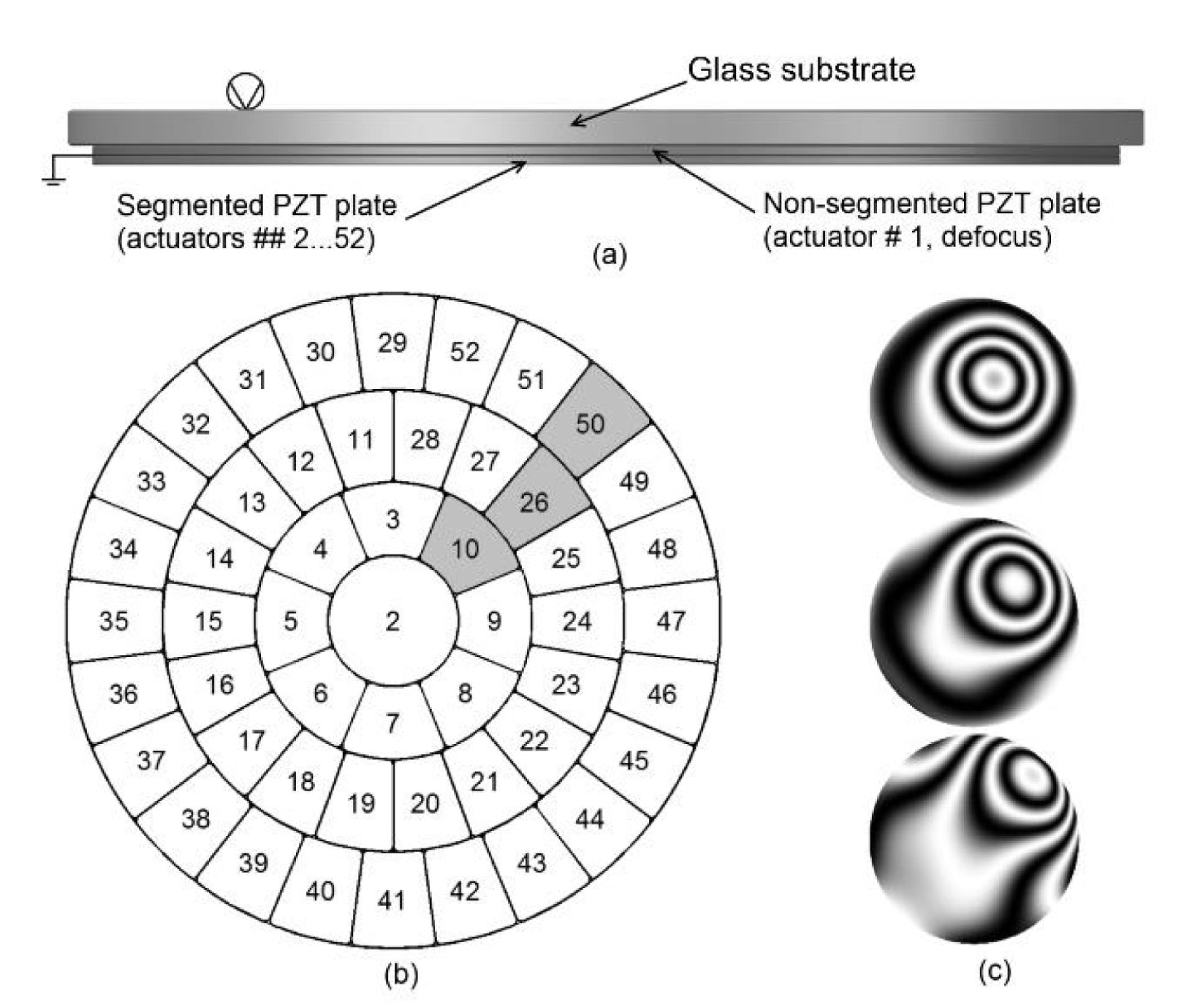
    Fig. 1. Design of the semi-passive bimorph mirror.
    Electrode pattern of the bimorph mirror $260~\text{mm}\times 260~\text{mm}$.
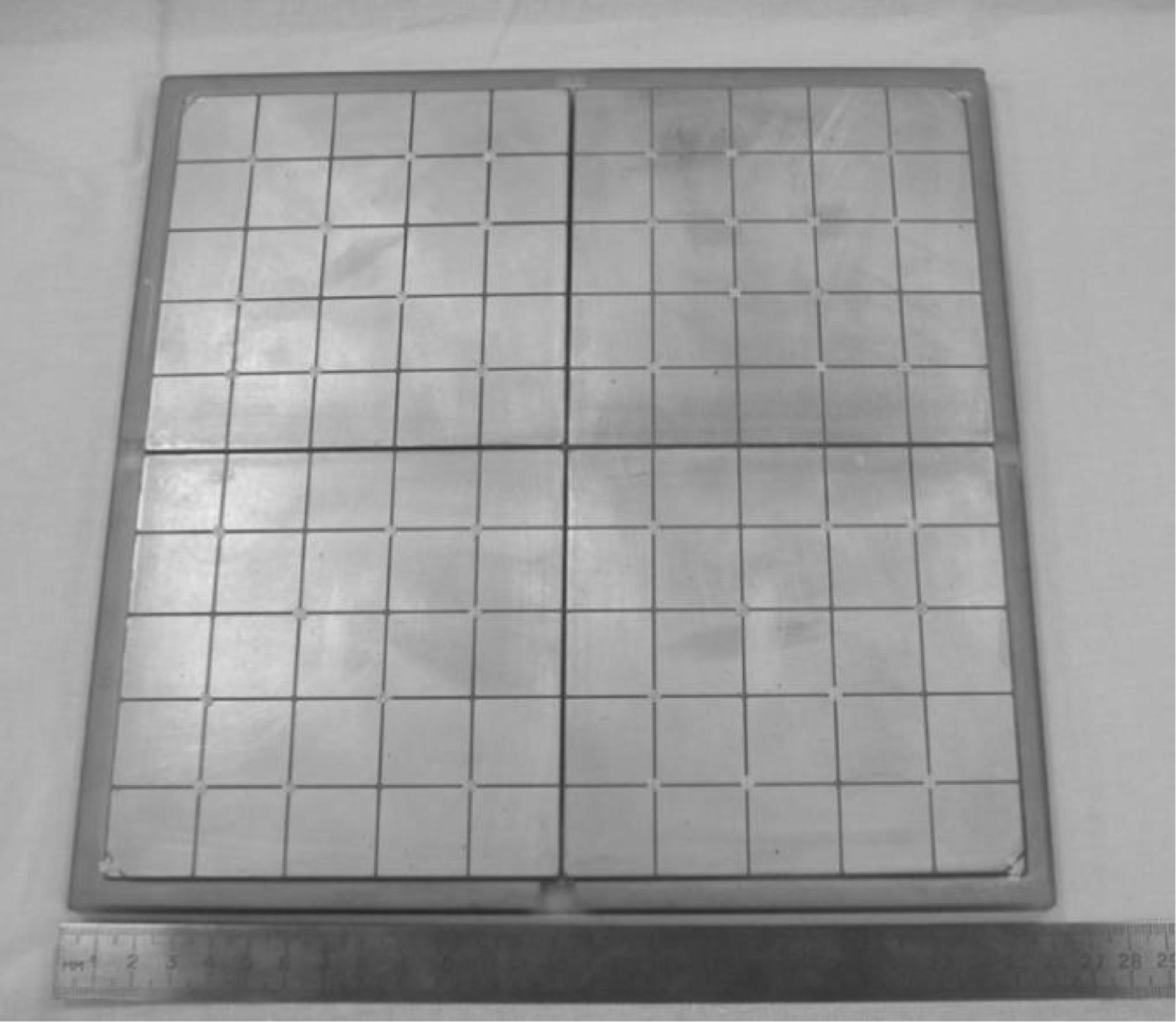
    Fig. 2. Electrode pattern of the bimorph mirror $260~\text{mm}\times 260~\text{mm}$.
    Photo of the bimorph deformable mirror $260~\text{mm}\times 260~\text{mm}$ attached in its mounting.
    Fig. 3. Photo of the bimorph deformable mirror $260~\text{mm}\times 260~\text{mm}$ attached in its mounting.
    Focal spot of the output laser beam: (a) before correction and (b) after correction of the wavefront; 11 and 1.3 diffraction limited sizes correspondingly.
    Fig. 4. Focal spot of the output laser beam: (a) before correction and (b) after correction of the wavefront; 11 and 1.3 diffraction limited sizes correspondingly.
    Layout and configuration of the electrodes.
    Fig. 5. Layout and configuration of the electrodes.
    Photo of the piezoelectric actuator.
    Fig. 6. Photo of the piezoelectric actuator.
    Combined deformable mirror: 1 – substrate with a reflective coating, 2 – actuators, 3 – metallic base.
    Fig. 7. Combined deformable mirror: 1 – substrate with a reflective coating, 2 – actuators, 3 – metallic base.
    Optical scheme for the analysis of the surface of the deformable mirror: 1 – 4-inch interferometer; 2–4 – folding mirrors; 5 – $6\times$ beam expander; 6, 7 – reference surfaces; 8 – deformable mirror; 9 – beam splitter; 10 – scaling telescope; 11 – Shack–Hartmann wavefront sensor; 12 - computer with software; 13 – electronic control unit for deformable mirror.
    Fig. 8. Optical scheme for the analysis of the surface of the deformable mirror: 1 – 4-inch interferometer; 2–4 – folding mirrors; 5 – $6\times$ beam expander; 6, 7 – reference surfaces; 8 – deformable mirror; 9 – beam splitter; 10 – scaling telescope; 11 – Shack–Hartmann wavefront sensor; 12 - computer with software; 13 – electronic control unit for deformable mirror.
    Flatness of the surface of the deformable mirror measured by wavefront sensor: (a) corrected only using the piezoelectric stack actuators ($1.517~{\rm\mu}\text{m}$ (P-V) and $0.377~{\rm\mu}\text{m}$ (RMS)); (b) corrected using also the bimorph electrodes ($0.162~{\rm\mu}\text{m}$ (P-V) and $0.033~{\rm\mu}\text{m}$ (RMS)); (c) map of control voltage applied both to stacked actuators and bimorph electrodes to flatten of the surface.
    Fig. 9. Flatness of the surface of the deformable mirror measured by wavefront sensor: (a) corrected only using the piezoelectric stack actuators ($1.517~{\rm\mu}\text{m}$ (P-V) and $0.377~{\rm\mu}\text{m}$ (RMS)); (b) corrected using also the bimorph electrodes ($0.162~{\rm\mu}\text{m}$ (P-V) and $0.033~{\rm\mu}\text{m}$ (RMS)); (c) map of control voltage applied both to stacked actuators and bimorph electrodes to flatten of the surface.
    Flatness of the surface of the deformable mirror, corrected using also the bimorph electrodes ($0.280{\it\lambda}$ (P-V) and $0.058{\it\lambda}$ (RMS) @ ${\it\lambda}=0.632~{\rm\mu}\text{m}$) measured with a ZYGO interferometer.
    Fig. 10. Flatness of the surface of the deformable mirror, corrected using also the bimorph electrodes ($0.280{\it\lambda}$ (P-V) and $0.058{\it\lambda}$ (RMS) @ ${\it\lambda}=0.632~{\rm\mu}\text{m}$) measured with a ZYGO interferometer.
    Point spread function of the corrected deformable mirror surface calculated by the ZYGO interferometer software – the estimated Strehl ratio is equal to 0.859.
    Fig. 11. Point spread function of the corrected deformable mirror surface calculated by the ZYGO interferometer software – the estimated Strehl ratio is equal to 0.859.
    Wavefront distortions of the output beam: (a) before correction and (b) after correction by means of wide aperture bimorph deformable mirror; (c) voltage map on the bimorph and stacked actuators of the mirror to correct of the wavefront distortions.
    Fig. 12. Wavefront distortions of the output beam: (a) before correction and (b) after correction by means of wide aperture bimorph deformable mirror; (c) voltage map on the bimorph and stacked actuators of the mirror to correct of the wavefront distortions.
    Vadim Samarkin, Alexander Alexandrov, Gilles Borsoni, Takahisa Jitsuno, Pavel Romanov, Aleksei Rukosuev, Alexis Kudryashov. Wide aperture piezoceramic deformable mirrors for aberration correction in high-power lasers[J]. High Power Laser Science and Engineering, 2016, 4(1): 010000e4
    Download Citation