• Photonics Research
  • Vol. 9, Issue 4, 535 (2021)
Xi Wang1、†, Weihong Shen2、†, Wenxiang Li1, Yingjie Liu1, Yong Yao1, Jiangbing Du2、3、*, Qinghai Song1, and Ke Xu1、4、*
Author Affiliations
  • 1Department of Electronic & Information Engineering, Harbin Institute of Technology, Shenzhen 518055, China
  • 2State Key Laboratory of Advanced Optical Communication Systems and Networks, Shanghai Jiao Tong University, Shanghai 200240, China
  • 3e-mail: dujiangbing@sjtu.edu.cn
  • 4e-mail: kxu@hit.edu.cn
  • show less
    DOI: 10.1364/PRJ.417107 Cite this Article Set citation alerts
    Xi Wang, Weihong Shen, Wenxiang Li, Yingjie Liu, Yong Yao, Jiangbing Du, Qinghai Song, Ke Xu. High-speed silicon photonic Mach–Zehnder modulator at 2 μm[J]. Photonics Research, 2021, 9(4): 535 Copy Citation Text show less
    Cross-sectional schematic diagram of the MZM’s active arms.
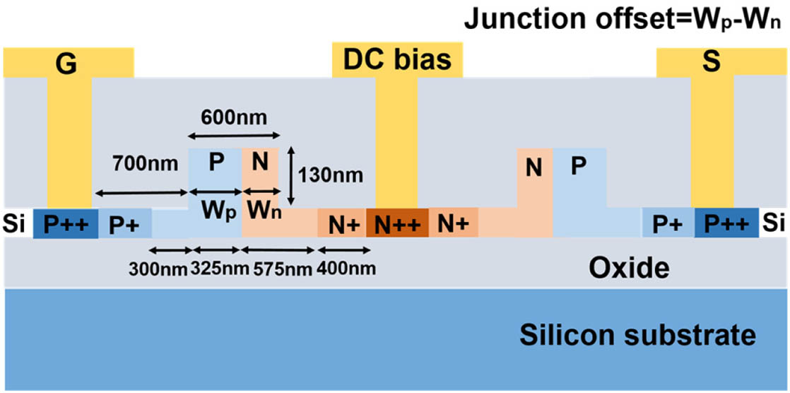
    Fig. 1. Cross-sectional schematic diagram of the MZM’s active arms.
    (a) Mode analysis of a rib waveguide with 90 nm slab thickness; the inset is the quasi-TE mode profile; (b) simulated optical loss at wavelength of 1950 nm.
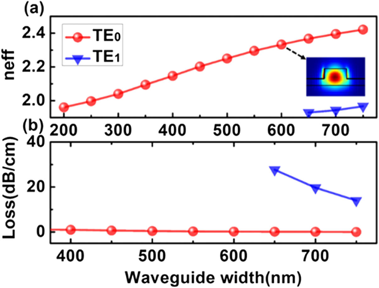
    Fig. 2. (a) Mode analysis of a rib waveguide with 90 nm slab thickness; the inset is the quasi-TE mode profile; (b) simulated optical loss at wavelength of 1950 nm.
    (a) Loss performance under different PN junction offsets at the voltage of 0 V, 2 V, and 4 V; (b) relationship between Lπ and PN junction offset under a voltage of 2 V and 4 V, respectively; (c) and (d) loss versus intermediate doping separation and heavy doping separation with a voltage of 0 V, 2 V, and 4 V, respectively.
    Fig. 3. (a) Loss performance under different PN junction offsets at the voltage of 0 V, 2 V, and 4 V; (b) relationship between Lπ and PN junction offset under a voltage of 2 V and 4 V, respectively; (c) and (d) loss versus intermediate doping separation and heavy doping separation with a voltage of 0 V, 2 V, and 4 V, respectively.
    Depletion width as a function of reverse bias. The inset is the distribution of electrons in the waveguide with a voltage of 0 V, 2 V, and 4 V, respectively.
    Fig. 4. Depletion width as a function of reverse bias. The inset is the distribution of electrons in the waveguide with a voltage of 0 V, 2 V, and 4 V, respectively.
    (a) Two-dimensional schematic diagram of T-shaped rail electrode structure; (b) electro-electro (EE) S21 parameters of T-shaped traveling-wave electrode.
    Fig. 5. (a) Two-dimensional schematic diagram of T-shaped rail electrode structure; (b) electro-electro (EE) S21 parameters of T-shaped traveling-wave electrode.
    Simulated frequency dependent (a) microwave attenuation, (b) microwave index, (c) characteristic impedance, and (d) EO S21 parameters.
    Fig. 6. Simulated frequency dependent (a) microwave attenuation, (b) microwave index, (c) characteristic impedance, and (d) EO S21 parameters.
    Optical microscope image of the traveling-wave MZM.
    Fig. 7. Optical microscope image of the traveling-wave MZM.
    (a) Measured optical transmission and (b) phase shift as functions of reverse bias.
    Fig. 8. (a) Measured optical transmission and (b) phase shift as functions of reverse bias.
    Schematic diagram of the high-speed measurement setup. PD, photodetector; DSO, digital storage oscilloscope; AWG, arbitrary waveform generator; TDFA, thulium-doped fiber amplifier; PC, polarization controller.
    Fig. 9. Schematic diagram of the high-speed measurement setup. PD, photodetector; DSO, digital storage oscilloscope; AWG, arbitrary waveform generator; TDFA, thulium-doped fiber amplifier; PC, polarization controller.
    Eye diagram for MZM at data rate of 30 Gbit/s with OOK modulation.
    Fig. 10. Eye diagram for MZM at data rate of 30 Gbit/s with OOK modulation.
    BER curves at different modulation rates. Inset: the offline post-FFE eye diagrams of 80 Gbit/s (left) and 60 Gbit/s (right) PAM-4 signals.
    Fig. 11. BER curves at different modulation rates. Inset: the offline post-FFE eye diagrams of 80 Gbit/s (left) and 60 Gbit/s (right) PAM-4 signals.
    Measured EO S21 response of the 2-μm MZM at −2 V DC bias.
    Fig. 12. Measured EO S21 response of the 2-μm MZM at 2  V DC bias.
    DispersionnApnEpnAnnEn
    Coefficients2.28×10180.8411.91×10210.992
    AbsorptionαApαEpαAnαEn
    coefficients6.21×10201.1193.22×10201.149
    Table 1. Free-Carrier Dispersion and Absorption Coefficients
    Xi Wang, Weihong Shen, Wenxiang Li, Yingjie Liu, Yong Yao, Jiangbing Du, Qinghai Song, Ke Xu. High-speed silicon photonic Mach–Zehnder modulator at 2 μm[J]. Photonics Research, 2021, 9(4): 535
    Download Citation