
Xi Wang, Weihong Shen, Wenxiang Li, Yingjie Liu, Yong Yao, Jiangbing Du, Qinghai Song, Ke Xu, "High-speed silicon photonic Mach–Zehnder modulator at 2 μm," Photonics Res. 9, 535 (2021)
- Photonics Research
- Vol. 9, Issue 4, 535 (2021)
Abstract
1. INTRODUCTION
The continuously increasing demands for data capacity have been a primary concern in the fiber optical communication community. Multiple degrees of freedom, such as wavelengths, guiding modes, polarizations, and fiber cores, have been extensively exploited to maximize the transmission data capacity [1–5]. For all those techniques, the fundamental limit of fiber capacity is still approaching. The proposal for 2-μm optical communications offers an approach to circumvent the barriers between demands and state-of-the-art transmission techniques [6]. Owing to the much broader gain bandwidth of thulium-doped fiber amplifier (TDFA), a 2-μm wavelength range is potentially capable of supporting more wavelength channels than a 1.55-μm communication band [7]. In addition, the fiber attenuation can be optimized to 0.1 dB/km via a hollow core structure [8]. Experimental results for high-speed transmission have been demonstrated by several groups via discrete packaged components [9–16], but the current challenges associated with high-speed integrated modulators [17–20] and photodetectors still exist [6].
Given the fact that the well-established silicon photonics silicon-on-insulator (SOI) platform is transparent to 2-μm wavelengths, photonic integration at 2 μm is expected to prove a boon to device performance at 2 μm. Recently, growing research efforts have been devoted to building a comprehensive 2-μm wave band compatible library of optical components on silicon, such as grating couplers [21], resonators [22], arrayed waveguide gratings [23], modulators [24–26], photodetectors [27–29], switches [30], and mode multiplexers [31]. Though various functional elements have been demonstrated, the lack of high-speed and advanced modulators significantly hampers the progress of 2-μm optical communications. In fact, modulation in silicon waveguides offers intrinsic advantages such as a stronger free-carrier dispersion effect and weaker two-photon absorption compared with the C-band. The free-carrier modulation effect in silicon was first reported at 2-μm band with 3 Gbit/s, where the lumped electrode, parasite resistance, and capacitance limit the modulation speed [24]. More recently, the traveling-wave Mach–Zehnder modulators (MZMs) have been demonstrated, and the reported modulation speeds were 20 Gbit/s [25] and 50 Gbit/s [26]. Possibly due to the bandwidth, linearity, and efficiency constraints, multilevel modulation with advanced formats has not yet been achieved for 2-μm silicon modulators.
In this paper, we demonstrate a high-speed silicon MZM operated at 2-μm wave band. The device is designed in a single-ended push–pull configuration and is fabricated at a standard silicon photonic foundry. For the first time, to our knowledge, we demonstrate multilevel modulation in a silicon waveguide at 2-μm. A modulation speed of 80 Gbit/s using PAM-4 format is achieved, which is a record data rate.
Sign up for Photonics Research TOC. Get the latest issue of Photonics Research delivered right to you!Sign up now
2. MODULATOR DESIGN AND FABRICATION
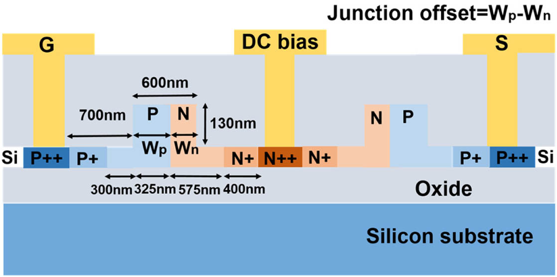
Figure 1.Cross-sectional schematic diagram of the MZM’s active arms.
![]()
Figure 2.(a) Mode analysis of a rib waveguide with 90 nm slab thickness; the inset is the quasi-TE mode profile; (b) simulated optical loss at wavelength of 1950 nm.
It is well known that the modulation in silicon waveguides mainly relies on the free-carrier dispersion effect. Both the real part and the imaginary part of the refractive index vary with the carrier concentration in the waveguide. This effect was quantitatively characterized in the 2-μm spectral range, and the results indicate the following relationship [33]:
Free-Carrier Dispersion and Absorption Coefficients
| Dispersion | ||||
| Coefficients | 0.841 | 0.992 | ||
| Absorption | ||||
| coefficients | 1.119 | 1.149 |
![]()
Figure 3.(a) Loss performance under different PN junction offsets at the voltage of 0 V, 2 V, and 4 V; (b) relationship between
To avoid the absorption loss from the doped region, we also optimize the separation between the waveguide and the electrodes by investigation of the loss and modulation efficiency under different gap distances. An intermediately doped region (N+) is designed to buffer between the waveguide and the electrode. The detailed parameters can be found in Fig. 1. The simulation results are plotted in Figs. 3(c) and 3(d). Though the intermediately doped slab has much weaker absorption than the electrode, a gap distance of 300 nm is chosen to ensure the loss level is below 2 dB/cm. This effect is much more significant for a heavily doped region. The loss can be substantially reduced when the gap distance becomes larger than 500 nm, even though too much separation between the heavily doped region and the waveguide is not suggested, since the serial resistance increases with the separation. Lower resistance is also desirable for larger bandwidth, which is mainly limited to the resistance-capacitance (RC) constant. Thus, the finalized gap distance is determined to be 700 nm, which corresponds to a loss level of
![]()
Figure 4.Depletion width as a function of reverse bias. The inset is the distribution of electrons in the waveguide with a voltage of 0 V, 2 V, and 4 V, respectively.
![]()
Figure 5.(a) Two-dimensional schematic diagram of T-shaped rail electrode structure; (b) electro-electro (EE)
![]()
Figure 6.Simulated frequency dependent (a) microwave attenuation, (b) microwave index, (c) characteristic impedance, and (d) EO
![]()
Figure 7.Optical microscope image of the traveling-wave MZM.
3. STATIC MEASUREMENTS
We first measure the DC response of the modulator. A narrow linewidth laser with an output wavelength of 1952 nm is used as the light source. A polarization controller is made of 5-m-long SM-1950 single-mode fiber and is used to ensure polarization alignment. A lensed fiber is used to focus the light into the edge coupler with a matched mode field diameter. The output from the chip is measured by an InGaAs power meter. DC voltage is applied onto the DC electrode pads via a pair of DC probes.
![]()
Figure 8.(a) Measured optical transmission and (b) phase shift as functions of reverse bias.
4. HIGH-SPEED MEASUREMENTS
![]()
Figure 9.Schematic diagram of the high-speed measurement setup. PD, photodetector; DSO, digital storage oscilloscope; AWG, arbitrary waveform generator; TDFA, thulium-doped fiber amplifier; PC, polarization controller.
![]()
Figure 10.Eye diagram for MZM at data rate of 30 Gbit/s with OOK modulation.
![]()
Figure 11.BER curves at different modulation rates. Inset: the offline post-FFE eye diagrams of 80 Gbit/s (left) and 60 Gbit/s (right) PAM-4 signals.
![]()
Figure 12.Measured EO
5. CONCLUSION
To summarize, we have experimentally demonstrated a silicon photonic MZM at 1950 nm with a single-ended push–pull configuration. The length of the modulator is 2 mm with a measured
References
[1] B. Zhu, T. Taunay, M. Fishteyn, X. Liu, S. Chandrasekhar, M. Yan, J. Fini, E. Monberg, F. Dimarcello. 112-Tb/s space-division multiplexed DWDM transmission with 14-b/s/Hz aggregate spectral efficiency over 76.8-km seven-core fiber. Opt. Express, 19, 16665-16671(2011).
[2] Z. Y. Chen, L. S. Yan, Y. Pan, L. Jiang, A. Yi, W. Pan, B. Luo. Use of polarization freedom beyond polarization-division multiplexing to support high-speed and spectral-efficient data transmission. Light Sci. Appl., 6, e16207(2017).
[3] D. J. Richardson, J. Fini, L. E. Nelson. Space-division multiplexing in optical fibres. Nat. Photonics, 7, 354-362(2013).
[4] S. Randel, R. Ryf, A. Sierra, P. Winzer, A. Gnauck, C. Bolle, R. Essiambre, D. Peckham, A. McCurdy, R. Lingle. 6×56-Gb/s mode division multiplexed transmission over 33-km few-mode fiber enabled by 6×6 MIMO equalization. Opt. Express, 19, 16697-16707(2011).
[5] L. Zhu, A. Wang, S. Chen, J. Liu, J. Wang. Orbital angular momentum mode multiplexed transmission in heterogeneous few-mode and multi-mode fiber network. Opt. Lett., 43, 1894-1897(2018).
[6] R. Soref. Enabling 2-μm communications. Nat. Photonics, 9, 358-359(2015).
[7] Z. Liu, Y. Chen, Z. Li, B. Kelly, R. Phelan, J. Carroll, T. Bradley, J. P. Wooler, N. V. Wheeler, A. M. Heidt, T. Richter, C. Schubert, M. Becker, F. Poletti, M. N. Petrovich, S. Alam, D. J. Richardson, R. Slavik. High-capacity directly modulated optical transmitter for 2-μm spectral region. J. Lightwave Technol., 33, 1373-1379(2015).
[8] P. J. Roberts, F. Couny, H. Sabert, B. J. Mangan, D. P. Williams, L. Farr, M. W. Mason, A. Tomlinson. Ultimate low loss of hollow-core photonic crystal fibres. Opt. Express, 13, 236-244(2005).
[9] K. Xu, L. Sun, Y. Q. Xie, Q. H. Song, J. B. Du, Z. Y. He. Transmission of IM/DD signals at 2-μm wavelength using PAM and CAP. IEEE Photon. J., 8, 7906407(2016).
[10] D. M. Kong, Y. Liu, Z. G. Ren, Y. M. Jung, M. H. Pu, K. Yvind, M. Galili, L. K. Oxenløwe, D. J. Richardson, H. Hu. Generation and coherent detection of 2-μm-band WDM-QPSK signals by on-chip spectral translation. Optical Fiber Communication Conference, M1I.4(2020).
[11] K. Xu, Q. Wu, Y. Xie, M. Tang, S. Fu, D. Liu. High speed single-wavelength modulation and transmission at 2-μm under bandwidth-constrained condition. Opt. Express, 25, 4528-4534(2018).
[12] M. N. Petrovich, F. Poletti, J. P. Wooler, A. M. Heidt, N. K. Baddela, Z. Li, D. R. Gray, R. Slavík, F. Parmigiani, N. V. Wheeler, J. R. Hayes, E. Numkam, L. G. Nielsen, B. Pálsdóttir, R. Phelan, B. Kelly, M. Becker, N. MacSuibhne, J. Zhao, F. C. G. Gunning, A. D. Ellis, P. Petropoulos, S. U. Alam, D. J. Richardson. First demonstration of 2-μm data transmission in a low-loss hollow core photonic bandgap fiber. Opt. Express, 21, 28559-28569(2013).
[13] Z. Li, A. M. Heidt, N. Simakov, Y. Jung, J. M. O. Daniel, S. U. Alam, D. J. Richardson. Diode-pumped wideband thulium-doped fiber amplifiers for optical communications in the 1800-2050 nm window. Opt. Express, 21, 26450-26455(2013).
[14] H. Zhang, N. Kavanagh, Z. Li, J. Zhao, N. Ye, Y. Chen, N. V. Wheeler, J. P. Wooler, J. R. Hayes, S. R. Sandoghchi, F. Poletti, M. N. Petrovich, S. U. Alam, R. Phelan, J. O’Carroll, B. Kelly, L. Grüner-Nielsen, D. J. Richardson, B. Corbett, F. C. G. Gunning. 100 Gbit/s WDM transmission at 2-μm: transmission studies in both low-cost hollow core photonic bandgap fiber and solid core fiber. Opt. Express, 23, 4946-4951(2015).
[15] W. Shen, J. Du, L. Sun, C. Wang, Y. Zhu, K. Xu, B. Chen, Z. He. Low-latency and high-speed hollow-core fiber optical interconnection at 2-micron waveband. J. Lightwave Technol., 38, 3874-3882(2020).
[16] W. Shen, P. Zeng, Z. Yang, D. Xia, J. Du, B. Zhang, K. Xu, Z. He, Z. Li. Chalcogenide glass photonic integration for improved 2-μm optical interconnection. Photon. Res., 8, 1484-1490(2020).
[17] P. Dong, L. Chen, Y. K. Chen. High-speed low-voltage single-drive push-pull silicon Mach-Zehnder modulators. Opt. Express, 20, 6163-6169(2012).
[18] X. Xiao, H. Xu, X. Y. Li, Z. Y. Li, T. Chu, Y. D. Yu, J. Z. Yu. High-speed, low-loss silicon Mach–Zehnder modulators with doping optimization. Opt. Express, 21, 4116-4125(2013).
[19] S. Z. Shao, J. F. Ding, L. C. Zheng, K. H. Zou, L. Zhang, F. Zhang, L. Yang. Optical PAM-4 signal generation using a silicon Mach-Zehnder optical modulator. Opt. Express, 25, 23003-23013(2017).
[20] Y. Y. Zhou, L. J. Zhou, H. K. Zhu, C. Y. Wong, Y. D. Wen, L. Liu, X. W. Li, J. P. Chen. Modeling and optimization of a single-drive push–pull silicon Mach–Zehnder modulator. Photon. Res., 4, 153-161(2016).
[21] J. Y. Li, Y. J. Liu, Y. Meng, K. Xu, J. B. Du, F. Wang, Z. Y. He, Q. H. Song. 2-μm wavelength grating coupler, bent waveguide, and tunable microring on silicon photonic MPW. IEEE Photon. Technol. Lett., 30, 471-474(2018).
[22] C. Luan, Y. Liu, Y. Ding, H. Hu. 2-μm high-speed graphene electro-optic modulator based on silicon slot microring resonator. Conference on Lasers and Electro-Optics, jTh2F.34(2020).
[23] Y. Liu, Z. Li, D. Li, Y. Yao, J. Du, Z. He, K. Xu. Thermo-optic tunable silicon arrayed waveguide grating at 2-μm wavelength band. IEEE Photon. J., 12, 4900308(2020).
[24] M. A. Camp, S. Assefa, D. M. Gill, T. Barwicz, S. M. Shank, P. M. Rice, T. Topuria, W. J. Green. Demonstration of electrooptic modulation at 2165 nm using a silicon Mach-Zehnder interferometer. Opt. Express, 20, 28009-28016(2012).
[25] W. Cao, D. Hagan, D. J. Thomson, M. Nedeljkovic, C. G. Littlejohns, A. Knights, S. Alam, J. J. Wang, F. Gardes, W. W. Zhang, S. H. Liu, K. Li, M. S. Rouifed, G. Xin, W. J. Wang, H. Wang, G. T. Reed, G. Z. Mashanovich. High-speed silicon modulators for the 2-μm wavelength band. Optica, 5, 1055-1062(2018).
[26] W. Li, M. Li, H. Zhang, Y. Zhang, H. Xie, X. Xiao, K. Xu. 50 Gbit/s silicon modulator operated at 1950 nm. Optical Fiber Communication Conference, M1D.4(2020).
[27] J. Guo, J. Li, C. Liu, Y. Yin, W. Wang, Z. Ni, Z. Fu, H. Yu, Y. Xu, Y. Shi, Y. Ma, S. Gao, L. Tong, D. Dai. High-performance silicon-graphene hybrid plasmonic waveguide photodetectors beyond 1.55 μm. Light Sci. Appl., 9, 29(2020).
[28] Y. Dong, W. Wang, S. Xu, D. Lei, X. Gong, X. Guo, H. Wang, S. Lee, W. Loke, S. Yoon, Y. Yeo. Two-micron-wavelength germanium-tin photodiodes with low dark current and gigahertz bandwidth. Opt. Express, 25, 15818-15827(2017).
[29] J. J. Ackert, D. J. Thomson, L. Shen, A. C. Peacock, P. E. Jessop, G. T. Reed, G. Z. Mashanovich, A. P. Knights. High-speed detection at two micrometres with monolithic silicon photodiodes. Nat. Photonics, 9, 393-396(2015).
[30] T. Yu, Y. J. Liu, Z. Y. Li, K. Xu, J. B. Du. Integrated thermo-optic switch for 2-μm spectral band. International Photonics and Opto-Electronics Meeting, OTu2B.4(2019).
[31] S. Zheng, M. Huang, X. Cao, L. Wang, Z. Ruan, L. Shen, J. Wang. Silicon-based four-mode division multiplexing for chip-scale optical data transmission in 2-μm waveband. Photon. Res., 7, 1030-1035(2019).
[32] D. Patel, S. Ghosh, M. Chagnon, A. Samani, V. Veerasubramanian, M. Osman, D. V. Plant. Design, analysis, and transmission system performance of a 41 GHz silicon photonic modulator. Opt. Express, 23, 14263-14287(2015).
[33] M. Nedeljkovic, R. Soref, G. Mashanovich. Free-carrier electrorefraction and electroabsorption modulation predictions for silicon over the 1–14 μm infrared wavelength range. IEEE Photon. J., 3, 1171-1180(2011).
[34] D. Frickey. Conversions between S, Z, Y, H, ABCD, and T parameters which are valid for complex source and load impedances. IEEE Trans. Microw. Theory Tech., 42, 205-211(1994).


Set citation alerts for the article
Please enter your email address

© Copyright 2018-2021 | Chinese Laser Press. All Rights Reserved 沪ICP备15018463号-20