
Ying Zeng, Weijun Wang, Furi Ling, Jianquan Yao. Terahertz wave modulation properties of thermally processed BST/PZT ferroelectric photonic crystals[J]. Photonics Research, 2020, 8(6): 1002
- Photonics Research
- Vol. 8, Issue 6, 1002 (2020)
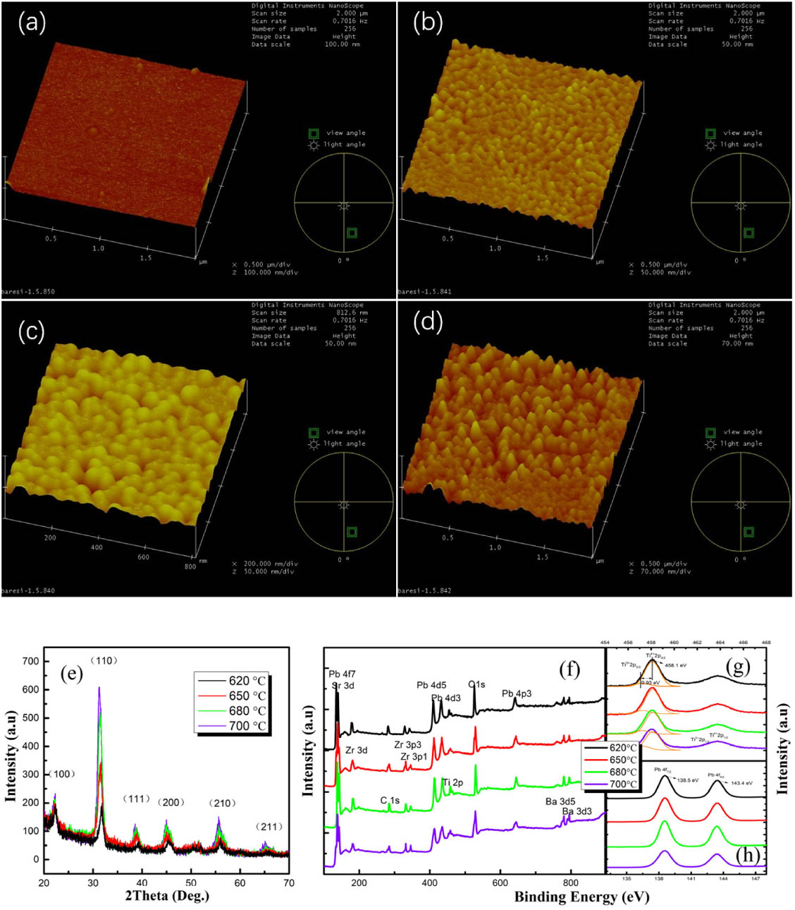
Fig. 1. AFM images of four samples annealed at: (a) 620°C, (b) 650°C, (c) 680°C, and (d) 700°C. The scan areas are 2 μm × 2 μm , 2 μm × 2 μm , 0.8 μm × 0.8 μm 2 μm × 2 μm
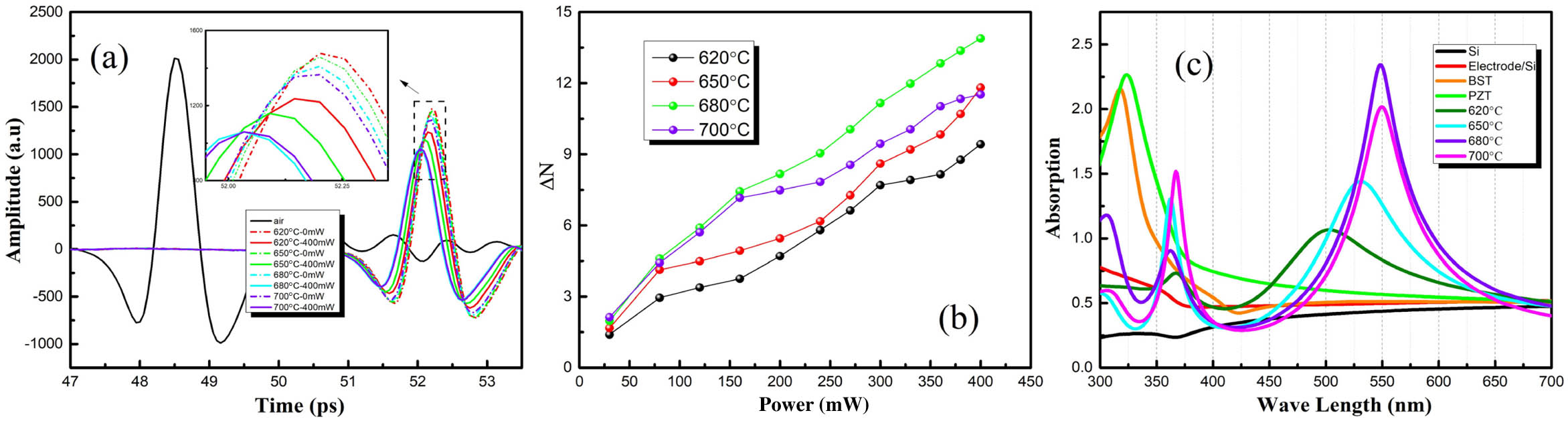
Fig. 2. (a) Time domain transmission spectrum of air; samples with 0 mW and 400 mW optical pump. (b) Power dependence of the refractive index variations of BST/PZT photonic crystals at 0.5 THz annealed at different temperatures. (c) UV-Vis absorption spectra of substrate (Si), substrate with electrode, BST, PZT monolayer, and BST/PZT photonic crystals annealed at different temperatures.
Fig. 3. Frequency dependence of the (a) real part and (b) imaginary part of dielectric permittivity of four samples annealed at different temperatures with 0 mW (spheres) and 400 mW optical pump power (stars). The data points are experimental values, and the solid lines are the fits by Eq. (2 ). (c) Raman spectra of four samples annealed at different temperatures. Pump power dependence of (d) dielectric permittivity and (e) loss tangent of four samples at 0.5 THz. (f) D–E loops of BST/PZT photonic crystals annealed at different temperatures measured at the electric field of 5000 kV/cm.
Fig. 4. Schematic diagrams of multi-field modulation processes of 680°C annealed sample: (a) pumped by static 532 nm optical field with dynamic electric field bias and (c) transmission modulation; (b) pumped by dynamic 532 nm optical field with static electric field bias and (d) transmission modulation; e , h , P e E o E o 1 , E o 2
| |||||||||||||||||||||||||||||
Table 1. Film Crystallinity, Lattice Parameter, and Grain Size of Four Samples Annealed at 620°C, 650°C, 680°C, and 780°C
| ||||||||||||||||||||||||||||||||||||||||||||||||||||||||||||||||||||||||||||||||||||||||||||||||||||||||||||||||||||
Table 2. Summary of Evaluated SM Parameters of BST/PZT Photonic Crystals with Different Annealing Temperaturesa
|
Table 3. Lowest-Frequency E(1TO) Phonon of BST/PZT Photonic Crystals with Different Annealing Temperatures in Fig. 3(c) Raman Spectra

Set citation alerts for the article
Please enter your email address
© Copyright 2018-2021 | Chinese Laser Press. All Rights Reserved 沪ICP备15018463号-20