Abstract
BST photonic crystals were fabricated by magnetron sputtering and annealed at . By controlling the crystallinity and the oxygen vacancies of the ferroelectric photonic crystals, the optically and electrically controllable terahertz wave modulations were realized. The variation in refractive index of the 680°C annealed sample showed the highest modulation to the optical pump and increased to 11.9 due to the highest absorption near 532 nm. In the optical pump, the electrons from ions could be stimulated and captured by ions, and the ratio of observed increased with the increasing annealing temperature, indicating the increasing oxygen vacancies concentration, which increased the 532 nm optical absorption and contributed to the improved optical modulation. The excess Pb migrating to the surface at higher annealing temperature might be one reason for the degradation of optical modulation. The increasing polarization and leakage current could contribute to the increasing permittivity and loss with the increasing annealing temperature. Two different results were observed on the sample annealed at 680°C when the order of applying external optical and electric fields was changed, due to the different migration mechanisms of excited carriers. This work provides a potentially effective approach to fabricate THz sensing, imaging, and communications devices with multi-function in the modulation of optical and electric multi-fields.
1. INTRODUCTION
In recent years, in order to achieve high modulation, a wide range of active materials have been explored for terahertz modulators, such as semiconductors (Si, Ge, GaAs) [1–4], liquid crystals [5], 2D materials (graphene, ) [6,7], superconductors [8], and phase change materials (, GeTe) [9,10]. Usually, these materials enable terahertz wave modulation by temperature modulation of electron mobility, electro-tuning Fermi level, or optically pumping electrons to achieve changes in conductivity. Most of these materials have a narrow bandgap and high intra-band electron mobility with obvious thermal effects, causing an unstable state and volatile response, especially under high-power electrical field or optical pumps. In addition, these materials usually respond to a single driving field, such as one of thermal, optical, or electrical stimulus. All of these hinder their applicability for multidimensional and high-power field modulation of terahertz waves.
In contrast, ferroelectric materials have advantages of possessing switchable electrical polarization, stable high dielectric properties, and remarkable electro-optical and nonlinear optical properties, and are used widely as actuators, transducers, sensors, energy and memory storage devices, among others [11–16]. Nevertheless, they are used mostly in microwave range by electrical or thermal control, because they can be effectively pumped only by ultraviolet [17,18] or X-rays [19] due to their wide bandgap. In order to narrow the bandgap, ferroelectric materials can be fabricated by controlling doping [20], fabrication conditions [21,22], thermal treatment [23,24], film thicknesses [25,26], and other methods [27,28]. These methods engineer the band structure mostly by changing oxygen vacancies and stresses. Oxygen vacancies have been a hot spot in recent years and used widely in perovskite materials for photocatalysis, energy storage, and solar fuel technologies [29–31]. In order to change the bandgap in a wider range, composite materials were proposed, one of which is photonic crystal. Advances in epitaxial growth techniques guaranteed the ferroelectricity and other properties in the extreme dimension [32,33] for nanoscale films, and also brought non-negligible and novel interfacial phenomena, such as enhanced dielectric properties [34], reduced leakage current [35], highly periodicity-dependent built-in electric field [36], tunable valley and spin polarizations [37], and lowered band gap and enhanced polarization [38].
Nevertheless, the exploration of ferroelectric material has been limited largely to visible and infrared frequencies, especially in terahertz range. Our intentions are to find the effects of different annealing temperatures on the surface morphology and structural, dielectric, and optical properties in the terahertz region and to obtain a fundamental understanding of relationships between the micro-structure and the properties for achieving an optimum processing for practical device applications. Our research on the annealing temperature effect and photonic crystal properties showed that the versatile and unique properties of ferroelectric materials allow for the realization of various terahertz functionalities such as thermally switchable multilevel nonvolatile states, and optically controllable and electrically driven light modulation. These unique features could be used in conjunction with each other and provide novel devices for efficient manipulation of terahertz waves.
Sign up for Photonics Research TOC. Get the latest issue of Photonics Research delivered right to you!Sign up now
In this work, we report a study of BST/PZT photonic crystals growing on Si substrates annealed at 620°C, 650°C, 680°C, and 700°C by terahertz spectroscopy with a 532 nm continuous-wave (CW) laser pump. The application of a sample annealed at 680°C under optical/electric multi-fields is also investigated.
2. EXPERIMENT
Preparation of samples. The samples of BST/PZT photonic crystals were prepared by radio frequency magnetron sputtering. The silicon crystals ([100] lattice orientation, electrical resistivity , thickness, -square) were used as substrates. The BST and PZT layers were grown with 20–30 nm/h deposition rate at 260°C with 100% Ar, by alternating the BST and PZT targets for three periods. Samples were annealed at 620°C, 650°C, 680°C, and 700°C for 10 min rapid thermal annealing.
Characterization. Thicknesses (BST 35.2 nm, PZT 36.7 nm for one period) were measured by a surface probe step meter (error of thickness values: 0.3 nm, vertical resolution: 0.001 nm). X-ray diffraction (XRD) was identified by an X-ray diffractometer (PANalytical PW3040-60 MRD). The surface morphology was tested by Veeco NanoScope MultiMode scanning probe microscopy. X-ray photoelectron spectroscopy (XPS) analysis was carried out using the AXIS-ULTRA DLD-600W instrument produced by Shimadzu-Kratos Company, Japan. The UV-Vis absorption spectra were obtained by a Lambda 35 UV-Vis spectrophotometer, produced by Perkin Elmer Company, USA. Raman spectra were achieved by a laser confocal Raman spectrometer (LabRAM HR800) produced by Horiba JobinYvon Company, France. The D–E loops were obtained at room temperature by the Precision Ferroelectric Tester system of Radiant Technologies, Inc.
Transmission spectra were measured by terahertz time-domain spectrometer (THz-TDS, which is produced by Zomega Terahertz Corporation, USA, 10 GHz frequency resolution, 3 mm diameter spot at the focus). An all-solid-state green (532 nm) CW laser was obliquely incident at an angle of 45° with the polar axis upon the surface of the sample, and the spot size was 5 mm in diameter. PZT film and BST film were in the ferroelectric and paraelectric phases at 18°C room temperature. In addition, a sample of Si substrate was also measured to eliminate the optical pump influence on the substrate.
3. EXPERIMENTAL RESULTS AND DISCUSSION
Figures 1(a)–1(d) show the surface morphologies of four samples. The root mean square (RMS) roughnesses of the surfaces are 1.203, 2.379, 3.350, and 6.976 nm for samples annealed at 620°C, 650°C, 680°C, and 700°C, respectively. None of the surface morphologies of the samples has defects or cracks. These results guarantee smooth surfaces, reducing the pump and probe light scattering in THz-TDS.
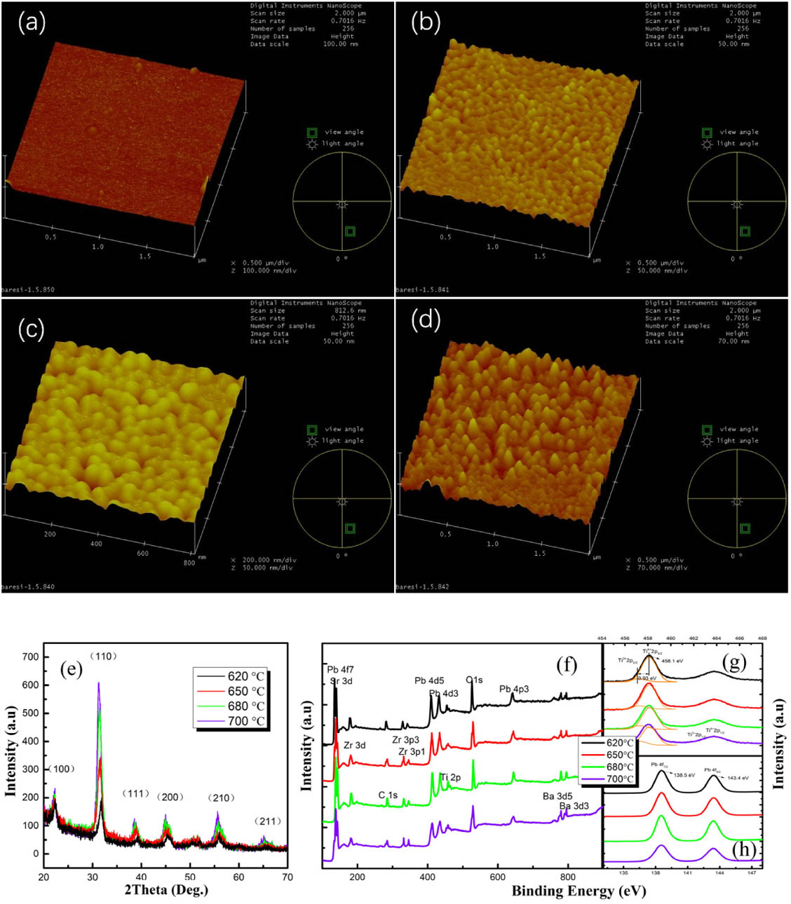
Figure 1.AFM images of four samples annealed at: (a) 620°C, (b) 650°C, (c) 680°C, and (d) 700°C. The scan areas are , and , correspondingly. (e) XRD spectra of four samples annealed at different temperatures. (f) XPS spectra of four samples annealed at different temperatures. (g) High-resolution Ti 2p XPS spectra; orange lines are the fitted Gaussian curves. (h) High-resolution Pb 4f XPS spectra.
The structural investigations of the samples were performed by XRD scan and are shown in Fig. 1(e) in a geometry from 20° to 70°. Mainly BST/PZT (100), (110), (200), and (210) peaks are observed, which clearly show the highly oriented crystallization of thin films on Si substrate. With the annealing temperature increasing, the (110) peaks of the perovskite phase of BST/PZT show distinct increase and become sharper.
To further analyze the lattice structure change by the annealing temperature, the film crystallinity, lattice parameter, and average grain size were calculated by XRD results and are listed in Table 1. It was found that three parameters were highly affected by the annealing temperature. To analyze the change caused by the annealing temperature, the crystallinity was defined as [39] . The crystallinity increased from 82.8% to 90.2% with the increasing annealing temperature, indicating the decrease in the impurity phase ratio. The increase in the lattice parameter could be attributed to the increasing interstitials (confirmed by XPS results later) caused by the increase in oxygen vacancies [40–42]. The electrons caused by the generation of oxygen vacancy hopped between different titanium ions in the perovskite structure, and then the ions captured the electrons and converted to ions. Because the radius of is larger than that of , it is clear that the reaction should be accompanied by a considerable volume expansion related to the appearance of . The more oxygen vacancies, the more ions generated, making the lattice constant increase with the increasing oxygen vacancy concentrations. The average grain size was found increasing with the increasing annealing temperature, which indicated the enhanced nucleation of the films. This could also contribute to the increase in the surface roughness observed in the atomic force microscope (AFM) results.
| Annealing Temperature (°C) | Crystallinity | Lattice Parameter (Å) | Average Grain Size (nm) |
| BST+PZT | BST | PZT | BST/PZT |
| 620 | 82.8% | 3.961 | 4.042 | 21 |
| 650 | 86.9% | 3.973 | 4.051 | 52 |
| 680 | 89.6% | 3.985 | 4.066 | 85 |
| 700 | 90.2% | 3.992 | 4.071 | 100 |
Table 1. Film Crystallinity, Lattice Parameter, and Grain Size of Four Samples Annealed at 620°C, 650°C, 680°C, and 780°C
Figures 1(f)–1(h) show XPS surface scanning spectra of BST/PZT photonic crystals at different annealing temperatures. The C peak assigned to the adventitious carbon was usually used as a reference for calibration. The XPS spectra in Fig. 1(f) confirmed the existence of Pb, Zr, Ti, O, Ba, Sr, and C elements. The high-resolution Ti 2p XPS spectra in Fig. 1(g) confirmed that four samples annealed at different temperatures were likely to have both and ions in the crystal lattice. The peaks of and were well fitted by Gaussian curves, and the binding energy of was lower than 458.1 eV of by 0.93 eV, which agreed with a former report [43]. In ferroelectric materials, oxygen vacancies can be easily formed by oxygen loss from the crystal lattice during the annealing process, due to the oxygen-reducing atmosphere or high annealing temperature according to the Kröger–Vink notation [44]. For perovskite structure ferroelectric materials such as PZT and BST, oxygen vacancies should be formed around to satisfy the requirement of charge equilibrium, . The ions could be partially reduced to by capturing the electrons created during the process described above, leading to an -type semiconducting nature with dielectric loss (leakage current). The ratio of calculated from the XPS results in Fig. 2(g) is 7.79%, 8.97%, 10.93%, and 12.91% [error less than 0.25%, , where and were the experimental intensity and the optimized fitting intensity of the Ti 2p XPS spectra in Fig. 1(g)], corresponding to the sample annealed at 620°C, 650°C, 680°C, and 700°C. These results indicated that the oxygen vacancies increased with the annealing temperature increasing.

Figure 2.(a) Time domain transmission spectrum of air; samples with 0 mW and 400 mW optical pump. (b) Power dependence of the refractive index variations of BST/PZT photonic crystals at 0.5 THz annealed at different temperatures. (c) UV-Vis absorption spectra of substrate (Si), substrate with electrode, BST, PZT monolayer, and BST/PZT photonic crystals annealed at different temperatures.
The above results show that the microstructure of the material changes with the annealing temperature. On this basis, we studied the terahertz wave modulation of photonic crystals with the annealing temperature.
A. Optical Properties
The terahertz time domain transmission spectra were observed changed in Fig. 2(a). This result indicated the optical and dielectric properties changed with the annealing temperature and the pump power. In order to explain the mechanism, the refractive index and the dielectric property of the BST/PZT photonic crystals were extracted by ( representing transmission) from the Fresnel format [45,46]. Figure 2(b) shows the variations in refractive index increasing with the annealing temperature increasing, indicating more free carriers were excited in the process of migration and diffusion. This can be illustrated as follows [47]: Here, , , represent the intensity of the optical pump power, refractive index, and linear electro-optical coefficient, respectively. , , , , are the space charge field and coefficient of dark irradiation, where represent the glass coefficient, photoionization section, acceptor concentration, electron charge, immigration rate of electrons, thermal emission rate, and photo excitation area, respectively. Among them, is likely to be greatly affected by annealing temperature and optical pump power. When applying an external optical field, the electrons in the illuminated area were excited and hopped to the conduction band. They migrated to the dark area, which led to a redistribution of carriers. The spatial redistribution of carriers led to an internal build-in charge field shielding the external field, and changed the samples’ refractive indices by the electro-optic effect in Fig. 2(b). The photon energy of the 532 nm CW laser for optical pump is about 2.3 eV, lower than the bandgaps of BST and PZT, which indicates the contribution of the excited free carriers from the sub-band.
To further confirm the existence of sub-bands, the UV-Vis absorption spectra were obtained. The absorption peaks of BST and PZT monolayers shown in Fig. 2(c) were at 318 nm and 324 nm, respectively, agreeing with previous studies [48,49]. Extra strong absorption peaks near 532 nm were observed in photonic crystals due to the Brillouin zone folding of the multilayer A/B periodic photonic crystals structure [50]. Oxygen vacancies have been reported to introduce a sub-band closely below the conduction band bottom, and this could contribute to the observed absorption peaks narrowing with a shift to the lower frequency [38,51]. This optical modulation process can be illustrated as follows: the Ti 3D electrons from the sub-band ( ions) in the illuminated area can hop to the conduction band [52]. They migrate to the dark area and then are captured by the trap level of . The enhanced crystallinity and PZT/BST interfacial effect with the increasing annealing temperature resulted in enhanced absorption of light energy. This led to the increased generation of carriers, which contributed to the improved optical modulation with the increasing annealing temperature. It is predictable that absorption peaks in other frequency domains can be obtained, not only at 532 nm. Samples of Si substrate and electrode/Si (in Fig. 4) were also tested and confirmed weak absorptions. These may provide references in the practical application of terahertz communication.
The highest absorption was observed in the sample annealed at 680°C. More free carriers could be excited due to the high absorption near 532 nm, which caused the maximum variation in refractive index for the sample annealed at 680°C according to Eq. (1). It is worth noting that there was a certain linewidth at the central frequency of the 532 nm laser; the total absorption should be the sum of the absorption in the linewidth. In the high-resolution XPS spectra of Pb in Fig. 2(h), the Pb peaks of the sample annealed at 700°C were clearly observed to decrease compared with the other three samples. This may be attributed to the excess Pb migrating to the surface in the fabrication process as reported in Ref. [53] and resulted in the decreasing variation in refractive index of the sample annealed at 700°C.
B. Dielectric Properties
In order to discuss the micro-mechanism of the change in optical properties, the THz-dielectric spectra in Figs. 3(a) and 3(b) were analyzed, and the coupled oscillator–relaxator model was applied [54]: where is the soft mode (SM) frequency, mainly of external field dependence; is the damping coefficient; is the oscillator strength; and are the bare relaxation frequency and strength of the central mode (CM), respectively; is the coupling coefficient; is the high-frequency permittivity. The evaluated SM parameters are listed in Table 2.
Figure 3.Frequency dependence of the (a) real part and (b) imaginary part of dielectric permittivity of four samples annealed at different temperatures with 0 mW (spheres) and 400 mW optical pump power (stars). The data points are experimental values, and the solid lines are the fits by Eq. (2). (c) Raman spectra of four samples annealed at different temperatures. Pump power dependence of (d) dielectric permittivity and (e) loss tangent of four samples at 0.5 THz. (f) D–E loops of BST/PZT photonic crystals annealed at different temperatures measured at the electric field of 5000 kV/cm.
| Pump Power (mW) | BST/PZT (620°C) | BST/PZT (650°C) | BST/PZT (680°C) | BST/PZT (700°C) |
| f | ωs | Γ | f | ωs | Γ | f | ωs | Γ | f | ωs | Γ |
| 0 | 4.4 | 74.3 | 7.5 | 5.4 | 72.6 | 12.5 | 6.8 | 70.9 | 19.7 | 7.7 | 68.5 | 24.7 |
| 80 | 5.4 | 74.6 | 9.6 | 6.9 | 72.9 | 19.6 | 8.8 | 71.3 | 23.6 | 9.7 | 69.1 | 25.6 |
| 160 | 5.9 | 76.0 | 15.3 | 7.7 | 76.9 | 33.1 | 10.3 | 72.3 | 47.1 | 11.3 | 70.4 | 41.1 |
| 240 | 6.8 | 76.9 | 20.6 | 8.6 | 78.1 | 39.4 | 11.7 | 75.5 | 60.6 | 12.6 | 75.1 | 52.5 |
| 320 | 8.1 | 78.8 | 25.6 | 10.5 | 80.3 | 45.1 | 14.2 | 78.5 | 70.5 | 15.1 | 78.4 | 63.5 |
| 400 | 9.6 | 82.0 | 31.5 | 12.9 | 81.3 | 52.4 | 17.2 | 79.2 | 85.4 | 18.1 | 79.3 | 83.4 |
| For CM, γ is 2.1−2.6, δ is 57−60, g is 5000. |
Table 2. Summary of Evaluated SM Parameters of BST/PZT Photonic Crystals with Different Annealing Temperaturesa
In order to confirm the accuracy of fitting results, Raman spectra of modes of the BST/PZT photonic crystals with different annealing temperatures were achieved and are shown in Fig. 3(c). One E mode and one mode came from the mode [55]. modes were active in tetragonal (4 mm) or rhombohedral (3 m) point groups stemming from the cubic representations. All the and modes were infrared and Raman active, while the mode was only Raman active. The lowest wave-number E(1TO) in the spectra originated from Pb/Ba/Sr ions vibrating against the octahedra network in the direction perpendicular to spontaneous polarization [56–58], and corresponded to the SM. With the oxygen vacancies increasing, localized vibrations associated with oxygen vacancies and the lack of translational symmetry contributed to the vibration frequency E(1TO) moving to a lower frequency [59,60]. With the annealing temperatures increasing, the perovskite phase developed. As a result, the strength of the Raman peaks of active modes increased, which was a good indication of the development of crystallinity for the PZT/BST perovskite phase [61,62]. E(1TO) frequency in Table 3 also agreed well with the fitting results at the 0 mW pump power in Table 2. This confirmed that the fitting results were accurate and could be used to analyze the optical pump state.
| Annealing Temperature (°C) | 620 | 650 | 680 | 700 |
| E(1TO) Frequency (cm−1) | 74.17 | 72.44 | 70.73 | 68.99 |
Table 3. Lowest-Frequency E(1TO) Phonon of BST/PZT Photonic Crystals with Different Annealing Temperatures in Fig. 3(c) Raman Spectra
To explain the photoinduced change of SM frequency, the field-induced SM variation is given as [63] where are the vacuum permittivity, fourth-order anharmonicity of the SM potential minimum, oscillator strength, initial value, spontaneous polarization, and built-in electric field, respectively. In Table 2, the SM frequencies of four samples increase with the increasing optical pump power. As previously illustrated, the external optical pump led to a carrier redistribution, formed a built-in electric field increasing with increasing pump power, and resulted in hardening of the SM according to Eq. (3). , also show noticeable increases in Table 2. In this case, is proportional to the number of oscillators , and are the effective charge, reduced mass, and vacuum permittivity, respectively. The damping coefficient was proportional to . Consequently, in the photonic crystals, the optical pump could cause the temperature increase, leading to increased , .
In Figs. 3(d) and 3(e), the dielectric permittivity and the loss tangent increased with the annealing temperature and the pump power increasing. To explain this phenomenon, confirming the variation of polarization and leakage current with annealing temperature is worthwhile.
Before D–E loops tests, about 50 nm conductive perovskite-structured metal oxide () layers were magnetron sputtered as top and bottom electrodes. This method not only ensured that the voltage could be applied to the photonic crystals by possessing good interface adhesion [64], but also ensured that the sample would not shield terahertz waves when applying the external electric field in further application (Fig. 4). Figure 3(f) shows D–E loops of BST/PZT photonic crystals measured at the electric field of 5000 kV/cm. The testing frequency is 10 Hz. The polarization of the photonic crystals is clearly observed increased in Fig. 3(f), which could be attributed to the increasing grain growth caused by increasing the annealing temperature [65]. The D–E loops became more and more typical when the annealing temperature decreased, which indicated that the leakage current decreased with the decreasing annealing temperature. These results indicate that enhanced nucleation and increasing oxygen vacancies could contribute to the increasing dielectric permittivity and loss, respectively [66].
Figure 4.Schematic diagrams of multi-field modulation processes of 680°C annealed sample: (a) pumped by static 532 nm optical field with dynamic electric field bias and (c) transmission modulation; (b) pumped by dynamic 532 nm optical field with static electric field bias and (d) transmission modulation; , and (including ) representing electrons, holes, electric field induced polarization, and built-in electric field induced by photo-generated carriers. Transmission modulation of 680°C annealed sample: (e) pumped by static 1064 nm optical field with dynamic electric field bias and (f) pumped by dynamic 1064 nm optical field with static electric field bias.
To illustrate the loss mechanism with the optical pump, the dielectric loss tangent was investigated. The results in Fig. 3(e) indicate that conduction loss plays a primary role in the entire loss, as conduction loss is well known to increase with the external field increasing [67]. Conduction loss is attributed mainly to three currents: the drift current [68], photovoltaic current [69], and diffusion current [70,71], where, are the elementary charge, mobility tensor, density of movable carriers, and electric field; are the photovoltaic tensor, components of the light wave, a real current constant, and light intensity; and are the Boltzmann constant and temperature, respectively. The temperature and free electrons generated by the optical pump are mainly pump power dependent, and these lead to increasing conduction loss with increasing pump power.
4. APPLICATION
Oxygen vacancy concentration can be tuned by annealing temperature, then modulating the sub-band gap of photonic crystals, and ultimately different modulations of terahertz waves can be achieved. Based on the above results, the 680°C annealed sample showed the highest modulation of dielectric and optical properties. Consequently, it was chosen to modulate a terahertz wave with 532 nm optical/direct-current (DC) electric multi-fields to discover its potential in practical application.
It was believed that there were two ways to change the transmissions in these processes: the change in carrier concentration caused by the optical pump, and the polarization caused by an external electric field. The electric field was not high enough to pump the carriers, but could make the carriers move in the electric field direction or form polarization. Multiple modulations of electric field and optical field will result in different distributions of photogenerated carriers, changes in polarization field, and the coupling between them. Therefore, different modulation results were achieved, as shown in Fig. 4. The residual total transmittance after sputtering top and bottom electrodes with a thickness of 50 nm was about 82.1%.
To describe the experimental process and explain the mechanism of the phenomena, schematic diagrams are shown in Fig. 4(a); we maintained the optical pump with constant power intensity in the electrical modulation process. As shown in Figs. 4(a) (i)–(iii), the applied voltage promoted the migration of electrons in the bright area to the dark area, and thus enhanced the carrier diffusion caused by concentration difference. This redistribution finally balanced because the carrier concentration was a function of the optical pump power. Then, only the polarization increased with the increasing electric field in Fig. 4(a) (iv). As a result, the transmission modulation [|transmission (50 V) − transmission (0 V)|/transmission (0 V)] increased from 9.8% to 25.1% with the increasing optical pump power in Fig. 4(c). In Fig. 4(b), we maintained DC electric field in the optical modulation process. As shown in Fig. 4(b) (i)–(iii), the polarization formed when applying the DC electric field and then was depolarized by the built-in electric field due to the redistribution of photo-generated carriers when applying the optical field. The carrier migration in vertical direction came to be stable when the polarization vanished with the increasing optical pump power. After that, the increasing photo-generated carrier would distribute only in the horizontal direction, as shown in Fig. 4(b) (iv). Since the polarization increased with the DC electric field, the carrier migration in vertical direction was enhanced. As a result, the migration in horizontal direction reduced, which led to a decrease in transmittance variation with the optical pump power when the electric field increased. Thus, the transmission modulation [|transmission (400 mW) − transmission (0 mW)|/transmission (0 mW)] decreased from 24.7% to 5.5% with the increasing DC field in Fig. 4(d).
In order to confirm the role of photo-generated carriers in the multi-field modulation process, the modulation of the 680°C annealed sample with 1064 nm optical/DC electric multi-fields was obtained.
Figures 4(e) and 4(f) show the transmission modulation of different orders of applying optical field and electric field. There was no significant difference between the results in Figs. 4(e) and 4(f), since a 1064 nm laser cannot pump a large number of photo-generated carriers. This result confirmed that the different couplings of the photo-generated carriers and the polarization played a significant role in 532 nm-optical/DC electric multi-field modulation.
5. CONCLUSION
BST/PZT photonic crystals were achieved by magnetron sputtering and annealed at four different temperatures of 620°C, 650°C, 680°C, and 700°C. The optical and electrical controllable terahertz wave modulations were achieved. In the optical pumping process, the variations in refractive index were attributed to an increased built-in electric field caused by carrier redistribution. Different annealing temperatures changed the oxygen vacancies concentration of photonic crystals, which directly resulted in different sub-band gaps and absorption. Polarization was observed to increase with the annealing temperature increasing due to the enhanced nucleation, as well as the leakage current due to the increasing oxygen vacancies. The degradation of optical modulation for a 700°C annealed sample was likely because excess Pb migrated to the surface at a higher annealing temperature. The loss of the 680°C annealed sample was observed to increase with the increasing external field due mainly to conduction loss. The 680°C annealed sample was chosen to modulate a terahertz wave with optical/electric multi-fields. Two different results were observed due to the different carrier migration processes. The results in this paper provide a reference for THz devices controlled by external fields.
Acknowledgment
Acknowledgment. We thank Guang Huang, engineer in the Center of Micro-Fabrication and Characterization (CMFC) of WNLO, for support in preparation of the samples, and thank the Analytical and Testing Center (ATC) of WNLO for support in testing of the samples.
References
[1] H. He, M. Yin, Z. Fu, Y. Lu, Q. Huang, H. Cai, Y. Zhao, X. Lin, H. Cheng. Ultrafast and broadband terahertz modulator with polarization selectivity. IEEE Photon. J., 11, 5901110(2019).
[2] S. A. Baig, J. L. Boland, D. A. Damry, H. H. Tan, C. Jagadish, H. J. Joyce, M. B. Johnston. An ultrafast switchable terahertz polarization modulator based on III-V semiconductor nanowires. Nano Lett., 17, 2603-2610(2017).
[3] X. Deng, M. Simanullang, Y. Kawano. Ge-core/a-Si-shell nanowire-based field-effect transistor for sensitive terahertz detection. Photonics, 5, 13(2018).
[4] C. Lange, T. Maag, M. Hohenleutner, S. Baierl, O. Schubert, E. R. Edwards, D. Bougeard, G. Woltersdorf, R. Huber. Extremely nonperturbative nonlinearities in GaAs driven by atomically strong terahertz fields in gold metamaterials. Phys. Rev. Lett., 113, 227401(2014).
[5] J. Wang, H. Tian, Y. Wang, X. Li, Y. Cao, L. Li, J. Liu, Z. Zhou. Liquid crystal terahertz modulator with plasmon-induced transparency metamaterial. Opt. Express, 26, 5769-5776(2018).
[6] M. Mittendorff, S. Li, T. E. Murphy. Graphene-based waveguide-integrated terahertz modulator. ACS Photon., 4, 316-321(2017).
[7] Y. Cao, S. Gan, Z. Geng, J. Liu, Y. Yang, Q. Bao, H. Chen. Optically tuned terahertz modulator based on annealed multilayer MoS2. Sci. Rep., 6, 22899(2016).
[8] C. Li, J. Wu, S. Jiang, R. Su, C. Zhang, C. Jiang, G. Zhou, B. Jin, L. Kang. Electrical dynamic modulation of THz radiation based on superconducting metamaterials. Appl. Phys. Lett., 111, 092601(2017).
[9] H.-F. Zhu, L.-H. Du, J. Li, Q.-W. Shi, B. Peng, Z.-R. Li, W.-X. Huang, L.-G. Zhu. Near-perfect terahertz wave amplitude modulation enabled by impedance matching in VO2 thin films. Appl. Phys. Lett., 112, 081103(2018).
[10] A. H. Gwin, C. H. Kodama, T. V. Laurvick, R. A. Coutu, P. F. Taday. Improved terahertz modulation using germanium telluride (GeTe) chalcogenide thin films. Appl. Phys. Lett., 107, 031904(2015).
[11] Z. W. Wei, J. Hu, W. Yu, T. Wu. Optically controlled electroresistance and electrically controlled photovoltage in ferroelectric tunnel junctions. Nat. Commun., 7, 10808(2016).
[12] Y. J. Shin, Y. Kim, S. J. Kang, H. H. Nahm, P. Murugavel, J. R. Kim, M. R. Cho, L. Wang, S. M. Yang. Interface control of ferroelectricity in an SrRuO3/BaTiO3/SrRuO3 capacitor and its critical thickness. Adv. Mater., 29, 1602795(2017).
[13] Y. Y. K. Xie, K. Yuan, W. Lu, K. Zhang, F. Xu, M. Ye, S. Ke, C. Shen, X. Zeng, X. Fan, B. Wei. Ferroelectric-enhanced polysulfide trapping for lithium-sulfur battery improvement. Adv. Mater., 29, 1604724(2017).
[14] M. R. Morris, S. R. Pendlebury, J. Hong, S. Dunn, J. R. Durrant. Effect of internal electric fields on charge carrier dynamics in a ferroelectric material for solar energy conversion. Adv. Mater., 28, 7123-7128(2016).
[15] X. Chen, X. Zhang, M. A. Koten, H. Chen, Z. Xiao, L. Zhang, J. E. Shield, P. A. Dowben, X. Hong. Interfacial charge engineering in ferroelectric-controlled Mott transistors. Adv. Mater., 29, 1701385(2017).
[16] W. Y. Kim, H. D. Kim, T. T. Kim, H. S. Park, K. Lee, H. J. Choi, S. H. Lee, J. Son, N. Park. Graphene-ferroelectric metadevices for nonvolatile memory and reconfigurable logic-gate operations. Nat. Commun., 7, 10429(2016).
[17] K. Song, N. Ma, Y. Yang. Enhanced self-powered UV photoresponse of ferroelectric PZT materials by pyroelectric effect. Adv. Mater. Technol., 2, 1700221(2017).
[18] N. Ma, Y. Yang. Enhanced self-powered UV photoresponse of ferroelectric BaTiO3 materials by pyroelectric effect. Nano Energy, 40, 352-359(2017).
[19] A. Chikina, M. Caputo, M. Naamneh, D. V. Christensen, T. Schmitt, M. Radovic, V. N. Strocov. X‐ray writing of metallic conductivity and oxygen vacancies at silicon/SrTiO3 interfaces. Adv. Funct. Mater., 29, 25(2019).
[20] K. Tang, R. Gu, S. Zhu, Z. Xu, J. Ye, S. Gu. Thermal evolution of zinc interstitial related donors in high-quality NH3-doped ZnO films. Opt. Mater. Express, 7, 593-605(2017).
[21] C.-K. Kao, C.-H. Tsai, I. N. Lin. Optical properties of Pb(Zr, Ti)O3 thin films on sapphire prepared by metalorganic decomposition process. Appl. Phys. Lett., 83, 3915-3917(2003).
[22] A. N. Morozovska, Y. M. Fomichov, P. Maksymovych, Y. M. Vysochanskii, E. A. Eliseev. Analytical description of domain morphology and phase diagrams of ferroelectric nanoparticles. Acta Mater., 160, 109-120(2018).
[23] Y. Liu, J. Liu, Y. Li, D. Wang, L. Ren, K. Zou. Effect of annealing temperature on the structure and properties of vanadium oxide films. Opt. Mater. Express, 6, 1552-1560(2016).
[24] D. Rasic, R. Sachan, J. Prater, J. Narayan. Structure-property correlations in thermally processed epitaxial LSMO films. Acta Mater., 163, 189-198(2019).
[25] E. D. Specht, H. M. Christen, D. P. Norton, L. A. Boatner. X-ray diffraction measurement of the effect of layer thickness on the ferroelectric transition in epitaxial KTaO3/KNbO3 multilayers. Phys. Rev. Lett., 80, 4317-4320(1998).
[26] S. Li, Y. L. Zhu, Y. L. Tang, Y. Liu, S. R. Zhang, Y. J. Wang, X. L. Ma. Thickness-dependent a1/a2 domain evolution in ferroelectric PbTiO3 films. Acta Mater., 131, 123-130(2017).
[27] G. J. Hu, X. K. Hong, J. H. Chu, N. Dai. Ferroelectric and optical properties of quasiperiodic PbZr0.5Ti0.5O3 multilayers grown on quartz wafers. Appl. Phys. Lett., 90, 162904(2007).
[28] S. Yoshida, K. Fujita, H. Akamatsu, O. Hernandez, A. Sen Gupta, F. G. Brown, H. Padmanabhan, A. S. Gibbs, T. Kuge. Ferroelectric Sr3Zr2O7: competition between hybrid improper ferroelectric and antiferroelectric mechanisms. Adv. Funct. Mater., 28, 1801856(2018).
[29] X. Sheng, T. Xu, X. Feng. Rational design of photoelectrodes with rapid charge transport for photoelectrochemical applications. Adv. Mater., 31, 1805132(2019).
[30] S. Wang, P. Chen, Y. Bai, J. H. Yun, G. Liu, L. Wang. New BiVO4 dual photoanodes with enriched oxygen vacancies for efficient solar-driven water splitting. Adv. Mater., 30, 1800486(2018).
[31] H. Zhu, M. Liu, Y. Zhang, Z. Yu, J. Ouyang, W. Pan. Increasing energy storage capabilities of space-charge dominated ferroelectric thin films using interlayer coupling. Acta Mater., 122, 252-258(2017).
[32] G. De Luca, N. Strkalj, S. Manz, C. Bouillet, M. Fiebig, M. Trassin. Nanoscale design of polarization in ultrathin ferroelectric heterostructures. Nat. Commun., 8, 1419(2017).
[33] P. Gao, Z. Zhang, M. Li, R. Ishikawa, B. Feng, H. J. Liu, Y. L. Huang, N. Shibata, X. Ma. Possible absence of critical thickness and size effect in ultrathin perovskite ferroelectric films. Nat. Commun., 8, 15549(2017).
[34] H. Khassaf, N. Khakpash, S. Vijayan, M. Aindow, S. P. Alpay. Electrostatically driven dielectric anomaly in mesoscopic ferroelectric-paraelectric bilayers. Acta Mater., 105, 68-74(2016).
[35] B. He, Z. Wang. Enhancement of the electrical properties in BaTiO3/PbZr0.52Ti0.48O3 ferroelectric superlattices. ACS Appl. Mater. Interfaces, 8, 6736-6742(2016).
[36] Q. Lin, D. Wang, Z. Chen, W. Liu, S. Lim, S. Li. Periodicity dependence of the built-in electric field in (Ba0.7Ca0.3)TiO3/Ba(Zr0.2Ti0.8)O3 ferroelectric superlattices. ACS Appl. Mater. Interfaces, 7, 26301-26306(2015).
[37] L. Yin, X. Wang, W. Mi. Tunable valley and spin polarizations in BiXO3/BiIrO3 (X = Fe, Mn) ferroelectric superlattices. ACS Appl. Mater. Interfaces, 10, 3822-3829(2018).
[38] Y. Zhang, M. P. Sahoo, J. Wang. Tuning the band gap and polarization of BaSnO3/SrSnO3 superlattices for photovoltaic applications. Phys. Chem. Chem. Phys., 19, 7032-7039(2017).
[39] J. H. Ma, X. J. Meng, J. L. Sun, T. Lin, F. W. Shi, G. S. Wang, J. H. Chu. Effect of excess Pb on crystallinity and ferroelectric properties of PZT(40/60) films on LaNiO3 coated Si substrates by MOD technique. Appl. Surf. Sci., 240, 275-279(2005).
[40] W. C. W. J. Kim, S. B. Qadri, J. M. Pond, S. W. Kirchoefer, D. B. Chrisey, J. S. Horwitz. Microwave properties of tetragonally distorted (Ba0.5Sr0.5)TiO3 thin films. Appl. Phys. Lett., 76, 1185-1187(2000).
[41] J. R. Petrie, C. Mitra, H. Jeen, W. S. Choi, T. L. Meyer, F. A. Reboredo, J. W. Freeland, G. Eres, H. N. Lee. Strain control of oxygen vacancies in epitaxial strontium cobaltite films. Adv. Funct. Mater., 26, 1564-1570(2016).
[42] U. Aschauer, R. Pfenninger, S. M. Selbach, T. Grande, N. A. Spaldin. Strain-controlled oxygen vacancy formation and ordering in CaMnO3. Phys. Rev. B, 88, 054111(2013).
[43] C. N. R. Rao, D. D. Sarma. Study of electron states of solids by techniques of electron spectroscopy. J. Solid. State. Chem., 45, 14-39(1982).
[44] C.-K. Chung, M. Lang, H. Xu, A. Navrotsky. Thermodynamics of radiation induced amorphization and thermal annealing of Dy2Sn2O7 pyrochlore. Acta Mater., 155, 386-392(2018).
[45] P. Kužel, F. Kadlec, J. Petzelt, J. Schubert, G. Panaitov. Highly tunable SrTiO3/DyScO3 heterostructures for applications in the terahertz range. Appl. Phys. Lett., 91, 232911(2007).
[46] V. Skoromets, C. Kadlec, J. Drahokoupil, J. Schubert, J. Hlinka, P. Kužel. Systematic study of terahertz response of SrTiO3 based heterostructures: influence of strain, temperature, and electric field. Phys. Rev. B, 89, 214116(2014).
[47] B. L.-D. Yuri, S. Kivshar. Dark optical solitons: physics and applications. Phys. Rep., 298, 81-197(1998).
[48] H. S. R. F. Tcheliebou, C. K. Hong, W. S. Park, S. Baik. On the microstructure and optical properties of Ba0.5Sr0.5TiO3 films. Thin. Solid. Films, 305, 30-34(1997).
[49] Z. Weihua, Z. Gaoyang, Z. Chen. Photosensitive PZT gel films and their preparation for fine patterning. Mater. Sci. Eng. B, 99, 168-172(2003).
[50] L. Zhang, Z. Xiong, L. Shan, L. Zheng, T. Wei, Q. Yan. Layer-by-layer approach to (2+1)D photonic crystal superlattice with enhanced crystalline integrity. Small, 11, 4910-4921(2015).
[51] K. Li, Z. Huang, X. Zeng, B. Huang, S. Gao, J. Lu. Synergetic effect of Ti3+ and oxygen doping on enhancing photoelectrochemical and photocatalytic properties of TiO2/g-C3N4 heterojunctions. ACS Appl. Mater. Interfaces, 9, 11577-11586(2017).
[52] A. Chikina, F. Lechermann, M. A. Husanu, M. Caputo, C. Cancellieri, X. Wang, T. Schmitt, M. Radovic, V. N. Strocov. Orbital ordering of the mobile and localized electrons at oxygen-deficient LaAlO3/SrTiO3 interfaces. ACS Nano, 12, 7927-7935(2018).
[53] S. B. Krupanidhi, H. Hu, V. Kumar. Multi‐ion‐beam reactive sputter deposition of ferroelectric Pb(Zr, Ti)O3 thin films. J. Appl. Phys., 71, 376-388(1992).
[54] C. Kadlec, V. Skoromets, F. Kadlec, H. Němec, J. Hlinka, J. Schubert, G. Panaitov, P. Kužel. Temperature and electric field tuning of the ferroelectric soft mode in a strained SrTiO3/DyScO3 heterostructure. Phys. Rev. B, 80, 174116(2009).
[55] P. S. Dobal, R. S. Katiyar. Studies on ferroelectric perovskites and bi-layered compounds using micro-Raman spectroscopy. J. Raman Spectrosc., 33, 405-423(2002).
[56] S. R. Shannigrahi, S. Tripathy. Micro-Raman spectroscopic investigation of rare earth-modified lead zirconate titanate ceramics. Ceram. Int., 33, 595-600(2007).
[57] M. Misra, K. Kotani, I. Kawayama, H. Murakami, M. Tonouchi. Observation of TO1 soft mode in SrTiO3 films by terahertz time domain spectroscopy. Appl. Phys. Lett., 87, 182909(2005).
[58] E. Buixaderas, V. Bovtun, M. Kempa, D. Nuzhnyy, M. Savinov, P. Vanek, I. Gregora, B. Malic. Lattice dynamics and domain wall oscillations of morphotropic Pb(Zr, Ti)O3 ceramics. Phys. Rev. B, 94, 054315(2016).
[59] Z. He, M. Cao, L. Zhou, L. Zhang, J. Xie, S. Zhang, J. Qi, H. Hao, Z. Yao. Origin of low dielectric loss and giant dielectric response in (Nb+Al) co-doped strontium titanate. J. Am. Ceram. Soc., 101, 5089-5097(2018).
[60] A. P. I. Taguchi, L. Wang, M. Proctor, F. Lévy, P. E. Schmid. Raman scattering study of lead zirconate titanate thin films prepared on silicon substrates by radio frequency magnetron sputtering. J. Appl. Phys., 74, 6625(1993).
[61] B. Jiang, Y. Tang, Y. Qu, J. Q. Wang, Y. Xie, C. Tian, W. Zhou, H. Fu. Thin carbon layer coated Ti3+-TiO2 nanocrystallites for visible-light driven photocatalysis. Nanoscale, 7, 5035-5045(2015).
[62] W. Zhu, Z. Q. Liu, M. S. Tse, T. S. Tan. Raman, FT-IR and dielectric studies of PZT 40/60 films deposited by MOD technology. J. Mater. Sci., 6, 369-374(1995).
[63] D. Nuzhnyy, J. Petzelt, S. Kamba, P. Kužel, C. Kadlec, V. Bovtun, M. Kempa, J. Schubert, C. M. Brooks. Soft mode behavior in SrTiO3/DyScO3 thin films: evidence of ferroelectric and antiferrodistortive phase transitions. Appl. Phys. Lett., 95, 232902(2009).
[64] Q. Yang, J. Cao, Y. Zhou, L. Sun, X. Lou. Dead layer effect and its elimination in ferroelectric thin film with oxide electrodes. Acta Mater., 112, 216-223(2016).
[65] J.-J. Choi, B.-D. Hahn, J. Ryu, W.-H. Yoon, D.-S. Park. Effects of Pb(Zn1/3Nb2/3)O3 addition and postannealing temperature on the electrical properties of Pb(ZrxTi1-x)O3 thick films prepared by aerosol deposition method. J. Appl. Phys., 102, 044101(2007).
[66] H. Deng, M. Zhang, Z. Hu, Q. Xie, Q. Zhong, J. Wei, H. Yan. Enhanced dielectric and ferroelectric properties of Ba and Ti co-doped BiFeO3 multiferroic ceramics. J. Alloy. Compd., 582, 273-276(2014).
[67] K. M. Johnson. Variation of dielectric constant with voltage in ferroelectrics and its application to parametric devices. J. Appl. Phys., 33, 2826-2831(1962).
[68] J. García, M. A. Mondragón, J. M. Hernández, J. L. Maldonado. Photocurrent determination of charge transport parameters in KNbO3:Fe3+. Opt. Mater., 3, 61-64(1994).
[69] H. H. G. Festl, P. Krätzig, E. R. von Baltz. Investigations of the photovoltaic tensor in doped LiNbO3. Phys. Status Solidi B, 113, 157-164(1982).
[70] M. Qin, K. Yao, Y. C. Liang, S. Shannigrahi. Thickness effects on photoinduced current in ferroelectric (Pb0.97La0.03)(Zr0.52Ti0.48)O3 thin films. J. Appl. Phys., 101, 014104(2007).
[71] V. G. Brovkovich, B. I. Siurman. Observation of nonequilibrium diffusion in LiNbO3 crystals. JETP Lett., 37, 550-553(1983).


