
Hui HUANG, Yi TIAN, Meng-die ZHANG, Tao-ran XU, Da MU, Pei-pei CHEN, Wei-guo CHU. Design and Batchable Fabrication of High Performance 3D Nanostructure SERS Chips and Their Applications to Trace Mercury Ions Detection[J]. Spectroscopy and Spectral Analysis, 2021, 41(12): 3782
- Spectroscopy and Spectral Analysis
- Vol. 41, Issue 12, 3782 (2021)
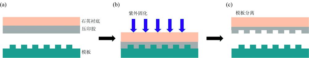
Fig. 1. Flow chart of NIL
(a): Immobilization of template and substrate; (b):Pressing and curing NIL resist;(c): Template-substrate separation for demolding
(a): Immobilization of template and substrate; (b):Pressing and curing NIL resist;(c): Template-substrate separation for demolding
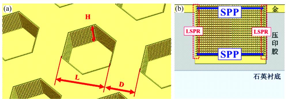
Fig. 2. (a) 3D isometric view of hexagonal nanopore/Au particle models (L =300 nm, D =200 nm, H =300 nm); (b) Schematic illustration (section view) of LSPR and SPP effects existing in each unit cell
Fig. 3. The effect of vertical configuration on the stress distribution
(a): 3D model of monolayer template; (b): 3D model of dual-layer template with a stress-homogenized zone; (c): Equivalent stress distribution on patterned area of monolayer template calculated by FEA method; (d): Equivalent stress distribution on patterned area of dual-layer template calculated by FEA method; (e): Equivalent stress distribution on 72% patterned area of monolayer template; (f): Equivalent stress distribution on 72% patterned area of dual-layer template; (g): Distribution diagram of low and high stress areas over patterns of the template; (h): Percentage stacked histogram of stress values of two models
(a): 3D model of monolayer template; (b): 3D model of dual-layer template with a stress-homogenized zone; (c): Equivalent stress distribution on patterned area of monolayer template calculated by FEA method; (d): Equivalent stress distribution on patterned area of dual-layer template calculated by FEA method; (e): Equivalent stress distribution on 72% patterned area of monolayer template; (f): Equivalent stress distribution on 72% patterned area of dual-layer template; (g): Distribution diagram of low and high stress areas over patterns of the template; (h): Percentage stacked histogram of stress values of two models
Fig. 4. (a—c) Schematic diagrams of dual-layer template with the size of (a) 7 mm, (b) 11 mm and (c) 15 mm;and their stress distributions (d—f) derived from FEA calculation, respectively
Fig. 5. Fabrication process and structure of template
(a): Three-dimensional flow chart of nanostructures convex on silicon template prepared by electron beam lithography, plasma enhanced reactive ion etching, lift-off process, etc; (b): Schematic diagram of the stress-homogenized zone on silicon template; (c)—(e): SEM images of hexagonal nanostructures of template
(a): Three-dimensional flow chart of nanostructures convex on silicon template prepared by electron beam lithography, plasma enhanced reactive ion etching, lift-off process, etc; (b): Schematic diagram of the stress-homogenized zone on silicon template; (c)—(e): SEM images of hexagonal nanostructures of template
Fig. 6. The photos of the quartz substrate surfaces after NIL using dual-layer templates with a size of (a) 15 mm, (b) 11 mm, (c) 7 mm and (d) using monolayer template with 7 mm side length; The lower right corner of each figure is the schematic diagram of executing template
Fig. 7. SEM images of hexagonal nanopore arrays with imprint resist on surface of a quartz substrate obtained by dual-layer template with a size of 7 mm
(a): Side view; (b): Vertical view; (c): Section view; (d): Side view after depositing Au nanoparticles
(a): Side view; (b): Vertical view; (c): Section view; (d): Side view after depositing Au nanoparticles
Fig. 8. Detection of R6G molecules by using SERS chips
(a): Raman spectra of R6G molecules with concentrations ranging from 1×10-11 to 1×10⁻⁵ mol·L-1 decorated on the SERS chips, respectively; (b): The calibration curves of the intensity of the peak at 1 360 cm-1 versus the logarithmic concentration for R6G molecules detection; (c): Bar graph of Raman intensity at 80 test points on SERS chip
(a): Raman spectra of R6G molecules with concentrations ranging from 1×10-11 to 1×10⁻⁵ mol·L-1 decorated on the SERS chips, respectively; (b): The calibration curves of the intensity of the peak at 1 360 cm-1 versus the logarithmic concentration for R6G molecules detection; (c): Bar graph of Raman intensity at 80 test points on SERS chip
Fig. 9. Hg ions detection by the SERS chips modified with bpy
(a): Raman spectra of Hg ions with different concentrations; (b): The relationship between Raman signal intensity (at 1 610 cm-1) and concentration of Hg ions
(a): Raman spectra of Hg ions with different concentrations; (b): The relationship between Raman signal intensity (at 1 610 cm-1) and concentration of Hg ions

Set citation alerts for the article
Please enter your email address
© Copyright 2018-2021 | Chinese Laser Press. All Rights Reserved 沪ICP备15018463号-20