• Chinese Optics Letters
  • Vol. 16, Issue 10, 101301 (2018)
Linjie Zhou*, Xinyi Wang, Liangjun Lu, and Jianping Chen
Author Affiliations
  • State Key Laboratory of Advanced Optical Communication Systems and Networks, Department of Electronic Engineering, Shanghai Jiao Tong University, Shanghai 200240, China
  • show less
    DOI: 10.3788/COL201816.101301 Cite this Article Set citation alerts
    Linjie Zhou, Xinyi Wang, Liangjun Lu, Jianping Chen. Integrated optical delay lines: a review and perspective [Invited][J]. Chinese Optics Letters, 2018, 16(10): 101301 Copy Citation Text show less
    Data synchronization and buffering in optical networks.
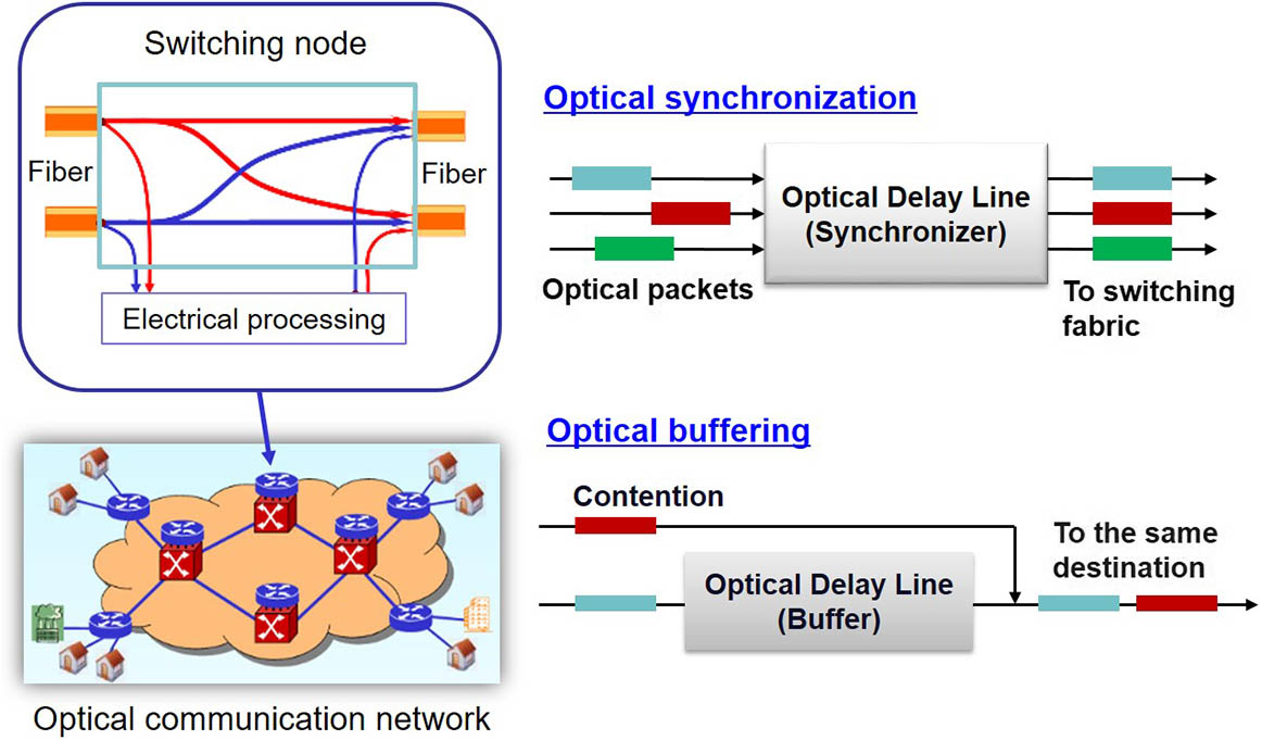
    Fig. 1. Data synchronization and buffering in optical networks.
    Photonics-assisted microwave beam forming and steering in phased array radar systems.
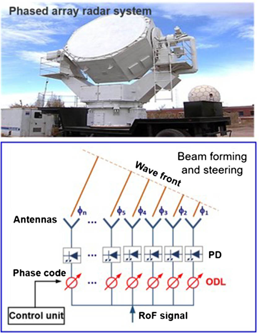
    Fig. 2. Photonics-assisted microwave beam forming and steering in phased array radar systems.
    Microwave photonic delay-line filter with a finite impulse response. PD, photodetector; VOA, variable optical attenuator; MUX, multiplexer; DEMUX, demultiplexer.
    Fig. 3. Microwave photonic delay-line filter with a finite impulse response. PD, photodetector; VOA, variable optical attenuator; MUX, multiplexer; DEMUX, demultiplexer.
    Typical system configuration of optical coherence tomography.
    Fig. 4. Typical system configuration of optical coherence tomography.
    Four-channel pulse interleaver using WDM-TDM implemented on a silicon chip[27].
    Fig. 5. Four-channel pulse interleaver using WDM-TDM implemented on a silicon chip[27].
    Three types of cascaded ring resonator delay lines: (a) SCISSOR; (b) CROW in transmission mode; (c) CROW in reflection mode.
    Fig. 6. Three types of cascaded ring resonator delay lines: (a) SCISSOR; (b) CROW in transmission mode; (c) CROW in reflection mode.
    Four types of integrated BGs with periodic modulation of (a) waveguide height, (b) waveguide width, (c) slab width, and (d) cladding.
    Fig. 7. Four types of integrated BGs with periodic modulation of (a) waveguide height, (b) waveguide width, (c) slab width, and (d) cladding.
    (a) Standard grating waveguide and its delay spectrum. (b) Cascaded complementary apodized gratings[74].
    Fig. 8. (a) Standard grating waveguide and its delay spectrum. (b) Cascaded complementary apodized gratings[74].
    BG delay line based on a 60-nm-thick silicon waveguide[35].
    Fig. 9. BG delay line based on a 60-nm-thick silicon waveguide[35].
    ODLs based on (a) chirped BG[73] and (b) linearly chirped contra-directional couplers with uniform BG[80].
    Fig. 10. ODLs based on (a) chirped BG[73] and (b) linearly chirped contra-directional couplers with uniform BG[80].
    ODL based on (a) line-defect PhCW and (b) coupled-cavity PhCW.
    Fig. 11. ODL based on (a) line-defect PhCW and (b) coupled-cavity PhCW.
    Schematics of the switchable ODLs in (a) parallel and (b) serial configurations.
    Fig. 12. Schematics of the switchable ODLs in (a) parallel and (b) serial configurations.
    1×N optical switches based on (a) cascaded 1×2 switch elements and (b) optical phased array.
    Fig. 13. 1×N optical switches based on (a) cascaded 1×2 switch elements and (b) optical phased array.
    (a) Architecture of the continuously tunable ODL structure; (b) mask layout of the ODL chip[110].
    Fig. 14. (a) Architecture of the continuously tunable ODL structure; (b) mask layout of the ODL chip[110].
    Recirculating loop delay line. (a) Integrated buffer; (b) gate matrix switch[113].
    Fig. 15. Recirculating loop delay line. (a) Integrated buffer; (b) gate matrix switch[113].
    Recirculating loop delay line in a parallel switchable configuration.
    Fig. 16. Recirculating loop delay line in a parallel switchable configuration.
    AWG-based wavelength-selective true-time-delay line. (a) Working principle illustration; (b) AWG layout.
    Fig. 17. AWG-based wavelength-selective true-time-delay line. (a) Working principle illustration; (b) AWG layout.
    Implementation of an ODL based on frequency-to-time mapping.
    Fig. 18. Implementation of an ODL based on frequency-to-time mapping.
    ODLsDelay Tuning Range (ps)Resolution (ps)Bandwidth (nm)Delay Loss (dB/ps)Power Efficiency (mW/ps)Footprint (mm2)
    SCISSORs[47]345Small>0.080.060.070.125
    CROWs[37]800Small0.020.010.155
    Grating[80]96Small0.80.001110.015
    PhCWs[91]54Small>30.17110.06
    4 bit SiN RTTDL[107]12350850Large1.9 × 10−40.023825
    Continuously tunable RTTDL[110]1280Small0.480.010.0528.62
    Wavelength-selective delay line[117]600400.40.011640
    Recirculating loop delay line[113]110020.00260
    MEMS[121]94Small0.040.24<0.001
    Table 1. Performance Comparison of Several Typical Integrated ODLs
    Linjie Zhou, Xinyi Wang, Liangjun Lu, Jianping Chen. Integrated optical delay lines: a review and perspective [Invited][J]. Chinese Optics Letters, 2018, 16(10): 101301
    Download Citation