State Key Laboratory of Advanced Optical Communication Systems and Networks, Department of Electronic Engineering, Shanghai Jiao Tong University, Shanghai 200240, China
Optical delay lines (ODLs) are one of the key enabling components in photonic integrated circuits and systems. They are widely used in time-division multiplexing, optical signal synchronization and buffering, microwave signal processing, beam forming and steering, etc. The development of integrated photonics pushes forward the miniaturization of ODLs, offering improved performances in terms of stability, tuning speed, and power consumption. The integrated ODLs can be implemented using various structures, such as single or coupled resonators, gratings, photonic crystals, multi-path switchable structures, and recirculating loop structures. The delay tuning in ODLs is enabled by either changing the group refractive index of the waveguide or changing the length of the optical path. This paper reviews the recent development of integrated ODLs with a focus on their abundant applications and flexible implementations. The challenges and potentials of each type of ODLs are pointed out.
1. INTRODUCTION
The physical nature of photons decides that optical signals cannot be stored directly inside a medium as electronic ones. At present, optical buffers are mostly realized in the form of optical delay lines (ODLs). The delay tuning is enabled either by slowing down the speed of light (via material dispersion or structural dispersion) or by switching to different lengths of waveguides[1,2]. Multiple practical applications require the ODLs to be continuously tunable and possess a broad operating bandwidth with a low insertion loss[3].
The ODLs can be implemented using bulk optics, fiber components, or integrated chips. Integrated on-chip ODLs exhibit multiple advantages compared to bulk optics or fiber-based ODLs, such as reduced cost, size, weight, and power consumption. The miniaturization of ODL components also improves the operation speed. In an integrated chip, the ODLs can be conveniently combined with other functional devices such as modulators, filters, lasers, and photodiodes, offering more powerful optical and microwave processing capabilities than a single component does.
Many different integration platforms can be utilized to make ODLs. A basic trade-off between the integration density and waveguide propagation loss needs to be considered before choosing the proper platform. The silica planar lightwave circuit (PLC) is a relatively mature platform for passive device integration. The refractive index contrast between core and cladding determines the waveguide cross-sectional dimension and the minimum bending radius. High index contrast () PLC waveguides have been employed to make compact devices[4]. The further increment of the refractive index contrast in silica PLC is limited by the stress in the doped silica core and upper cladding. Silicon nitride () and silicon oxynitride (SiON) are good alternatives for passive PLC due to their high index contrast and complementary metal–oxide–semiconductor (CMOS)-compatible fabrication process. The waveguide propagation loss can be below 0.1 dB/cm, providing excellent low-loss optical channels for most passive devices. Due to their material limitations, the silica and cannot be used to make active and high-speed optical components. On the other hand, indium phosphide (InP), as a traditional optoelectronic material, is suitable for monolithic integration of both active (such as lasers, photodiodes, modulators) and passive devices (such as waveguides, filters, splitters, combiners) on a single chip[5]. However, the monolithic integration tends to have significant compromise in the performance of each component due to the different requirements of the material composite for optimal performances. The manufacturing yield is another issue, since the breakdown of a single component would result in a failure of the entire chip. Silicon photonics is regarded as one of the most promising technologies for large-scale high-density photonic integration in recent years. Thanks to its large index contrast, the bending radius of a channel waveguide can be as small as 1–2 μm[6]. All kinds of passive devices, high-speed silicon modulators, and germanium photodiodes have been intensively investigated and have achieved great success in recent years[7]. The III–V lasers can be integrated onto the silicon photonic chip via hybrid bonding or epitaxial growth[8,9].
Sign up for Chinese Optics Letters TOC. Get the latest issue of Chinese Optics Letters delivered right to you!Sign up now
This review focuses on the various structures and technologies to realize integrated ODLs. Although there are a lot of other interesting works on ODLs or buffers implemented with new technologies, we only cover some representative work to illustrate the diversity and flexibility of integrated ODLs. The different integrated ODLs have their own pros and cons, and the selection should take into consideration the practical application requirements.
2. APPLICATIONS OF ODLs
A. Synchronization and Buffering
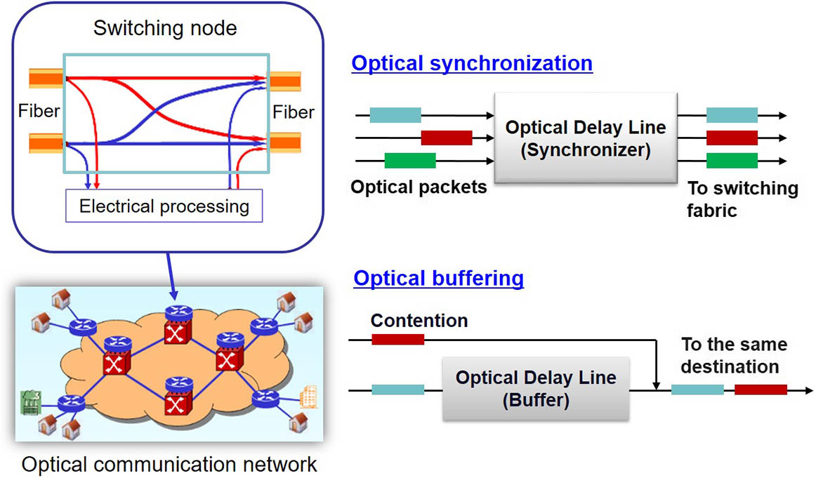
With the development of optical networks, more advanced and flexible fiber-optic systems employing all-optical routing are highly demanded, where optical signals must be directly processed in the optical layer. Multiple optical signal processing functions are demanded in the switching nodes of these networks, including matrix switch, signal regeneration, clock signal recovery, wavelength conversion, optical buffering, etc. As shown in Fig. 1, the optical buffers are key components in optical packet switching networks for resolving the packet contention in the optical domain and thus reducing packet loss rate without optic-electronic-optic (OEO) conversion. Early all-optical switching networks used electrical random-access memory (RAM) with OEO conversion, where the contention is resolved easily in the electrical domain. However, the OEO conversion makes the system very complex, and the system’s electrical power consumption is relatively large. The switching speed of this method is limited by the reading and writing speed of the electrical RAM. As a result, it is considered that the data buffering function should be accomplished completely in the optical domain without OEO conversion. As the electrical routers can no longer be further scaled, the optical packet switching technologies may soon manifest as an important technology in optical routers due to its efficient use of capacity and flexibility. However, it needs optical buffers to solve the contention and congestion issues within core routers. Unfortunately, there are no mature and feasible optical buffering solutions or devices. Therefore, the existing data buffering and synchronization functions are all based on various ODLs[10–12].
Figure 1.Data synchronization and buffering in optical networks.
The ODL-based buffers can also find applications in time-slot interchangers. In Ref. [13], the variable optical buffering stage utilizes silicon integrated ODLs and differentially biased semiconductor optical amplifier Mach–Zehnder interferometer (SOA-MZI)-based wavelength converters (WCs) for time-slot rearrangement. Time-slot interchange of 10 Gb/s optical packets has been demonstrated.
B. Optical Beamforming and Steering
Another important application area of the tunable ODLs is broadband photonic and microwave information processing, such as phased array antennas (PAAs) for optical beamforming networks (OBFNs)[14–18]. Owing to its high directivity and fast steering capability, the PAA has intrigued much research for high performance communication and radar systems in both civilian and military applications. Figure 2 shows the principle of microwave beamforming based on PAAs[19]. The PAA comprises multiple antenna units, each connected with a phase shifter at the back end. When the signal enters the transmitter, its phase is tuned by the phase shifter. Through tuning the relative phase between antenna units, microwaves in the desired frequency range are formed and directed to a desired direction. In the conventional electronic PAAs, the microwave phase shift is independent of frequency, leading to the beam squint effect. The optically beamformed PAA can effectively overcome the above-mentioned problem, in which the phase shifter is based on a tunable true-time ODL with a large tuning range and high accuracy. Moreover, it is advantageous in terms of microwave frequency tuning over a broadband and seamless integration with other photonic components. As the optical beamformer works bidirectionally, the same device can be used as transmitter and receiver simultaneously. The optical PAA can fulfill the growing demand for bandwidth requirements of the future broadband wireless access applications.
Figure 2.Photonics-assisted microwave beam forming and steering in phased array radar systems.
With the assistance of ODLs, microwave filters can be realized with a broadband response. Figure 3 shows the principle of implementing a finite impulse response (FIR) microwave photonic filter[20]. The optical carrier is a multi-wavelength comb source that could be generated using a microring resonator based on the degenerate four-wave mixing[21]. The microwave signal to be processed is modulated onto the optical carrier and is then divided in wavelength by a demultiplexer. The optical channels experience incremental delays in the ODLs and combine in another multiplexer. The microwave filtering function is realized after optical-to-electrical conversion in the photodiode. The microwave photonic filter can be modeled as a linear time-invariant (LTI) system. Its transfer function is determined by the optical power and delay of each optical tap. The low-loss variable ODL is an indispensable component in the tunable microwave filter.
Figure 3.Microwave photonic delay-line filter with a finite impulse response. PD, photodetector; VOA, variable optical attenuator; MUX, multiplexer; DEMUX, demultiplexer.
Fiber-based ODLs have been widely used in optical coherence tomography (OCT)[22]. The OCT is based on the low-coherence interferometry in a Michelson interferometer, as shown in Fig. 4. A broadband optical beam is divided into two arms with one as the reference arm and the other as the sample arm. The recombination of the reflective light from the reference and sample arms gives rise to an interference pattern only when the optical path difference between the two arms is within the optical coherent length. Any light outside the coherent length will not interfere but emerge as the background. The scanning depth of the sample is controlled by the ODL in the reference arm. The deep scanning, thus, requires the delay line to have a large tuning range. Meanwhile, in order to obtain a real-time OCT image, the ODL also needs to be fast tuned. Linearly chirped fiber Bragg gratings (BGs) can provide long variable delays yet with a much smaller size compared to single-mode fibers. The fiber ODLs are bulk components, suffering from the stability issue. They can be replaced by integrated delay lines based on dielectric waveguide circuits to make it more compact and stable[23].
Figure 4.Typical system configuration of optical coherence tomography.
Optical time-division multiplexing (TDM) is a straightforward application of ODLs in optical communications[24,25]. In TDM, the bit-rate of a serialized data stream is a multiplication of the bit-rate of an individual channel and the number of parallel channels, which greatly increases the transmission capacity of a single fiber-optic link. The ODL is used to adjust the temporal sequence of the input data streams during the parallel-to-serial conversion.
The TDM combined with wavelength-division multiplexing (WDM) can be used to increase the repetition rate of an input optical pulse train[26,27]. The high-speed pulse train is highly required in photonic analog-to-digital conversion (PADC) to increase the sampling rate. Figure 5 illustrates a four-channel time-wavelength optical pulse interleaver implemented on a silicon chip[27]. The input/output wavelength (de)multiplexer is implemented by arrays of microring resonator filters, and the delay lines are realized by long sections of silicon waveguides. The input pulse train is divided by the ring demultiplexers into four wavelengths. They experience linearly increasing delays in the ODL banks, before finally being multiplexed back into a single path. The resulted pulse repetition rate is four times higher than the initial input one. The delay values need to be precisely controlled in order to have a uniform spacing in the multiplexed pulses. The ODL insertion loss is also required to be small in order to suppress the pulse amplitude fluctuation. Alternatively, variable optical attenuators can be inserted in the ODL to equalize the amplitude of the WDM-divided pulses.
Figure 5.Four-channel pulse interleaver using WDM-TDM implemented on a silicon chip[27].
In addition to the several important applications mentioned above, there are many other applications for integrated ODLs in different areas. They can be used to build an integrated optical gyroscope. For instance, the gyroscope in Ref. [28] uses a 10-m-long single-layer waveguide. The waveguide spacing is 50 μm, and the entire ODL occupies an area smaller than . An integrated tunable ODL loaded in a Mach–Zehnder interferometer (MZI) works as a good receiver for differential phase shift keying (DPSK) optical transmission systems[29]. The continuous control of the MZI delay allows the optimization of the receiver performance for the detection of DPSK signals at variable symbol rates. Optoelectronic implementation of reservoir computing needs a single nonlinear node and a delay line as the key elements[30]. The bio-inspired approach is sufficiently fast for real-time information processing, comparable to state-of-the-art digital implementations. Other than PAAs and microwave photonic filters, the ODLs have a rich use in processing microwave signals. For instance, it can be employed in synthesizing of reconfigurable radio-frequency arbitrary waveforms[31]. The integrated on-chip optical delay elements offer an approach to accurately manipulating individual radio-frequency waveforms with higher speed and lower timing jitter than electronic methods.
3. DESIGN CONSIDERATIONS
The design of an integrated ODL needs to take into consideration the specific applications. It is quite challenging to get optimal performances in all aspects. Usually, a compromise has to be made in order to reach a certain performance. In general, the following several basic metrics need to be considered in designing an ODL.
A. Delay Tuning Range
The delay tuning range represents the difference between the minimum and the maximum delays that can be achieved. The maximum delay is usually limited by waveguide loss, group delay dispersion, or chip size. The minimum delay determines the minimum buffering capacity of the ODL. A nanosecond tuning range is achievable in most integration platforms, and this tuning range could already satisfy a lot of applications.
B. Delay Tuning Resolution
The requirement for delay tuning resolution is application dependent. For example, in phased array radar, the delay tuning resolution is related to the angle scanning step during beam steering. When used as an optical buffer in optical communication systems, it is related to the data rate of the system. A lot of ODL structures can provide continuous delay tuning, as long as the driving voltage is continuously varied. In practice, the delay fluctuation due to the drift of driving voltage and chip temperature may affect the attainable resolution.
C. Optical Bandwidth
In multiple ODL structures, the optical delay and bandwidth product is a constant value. A large delay is only obtained with the sacrifice of its bandwidth. A high-speed optical signal occupies a large bandwidth. The delay bandwidth needs to be large enough to ensure that the signal after ODL is not significantly distorted. Moreover, a broadband ODL can support WDM transmission, providing the multi-channel parallel processing capacity.
D. Insertion Loss
Low loss is the basic requirement for an ODL in most applications. The loss mainly comes from the waveguide propagation loss in passive ODLs. Tuning may bring additional loss either from the material absorption loss (e.g., free-carrier absorption) or from the structural loss (e.g., optical switches) in actively tunable ODLs. If the loss is too large, the optical signal must be boosted by using an optical amplifier in subsequent transmission, which increases the complexity and lowers the signal-to-noise ratio.
E. Power Consumption
One of the advantages of integrated devices over traditional discrete devices lies in their low power consumption. In optical routers or OBFNs, a large number of tunable ODLs are required, so the power consumption of the delay line will accumulate to a considerably large level, which in turn will affect its stability due to thermal crosstalk. The ODL therefore should be designed to have low tuning power consumption.
F. Size and Weight
In photonic devices, the size determines its integration density. The smaller the size, the better the ODL can be integrated with other devices in convenience and flexibility. The ODL device footprint is affected by multiple factors like minimum bending radius, maximum delay, delay tuning step, control electronics, and optical and thermal isolation.
4. IMPLEMENTATION METHODS
The tunable ODL plays a key role in all of the above-mentioned applications. Several schemes for realizing the tunable ODL can be obtained by examining light transmission in a dielectric waveguide. Assuming that light enters a waveguide with a propagation distance of L, and the effective refractive index of the waveguide is , the phase change of the lightwave is given by
Thus, the group delay suffered by the lightwave is
It can be seen from Eq. (2) that there are three methods to tune the group delay: change the effective refractive index of the waveguide;change the dispersion of the effective refractive index of the waveguide, that is, adjust the group refractive index;change the physical length of the waveguide.
The first method has a limited efficiency, because the effective refractive index of the waveguide is related to the core/cladding material refractive index and the waveguide cross-sectional structure. In fact, the variable range of delay is quite small, and it is hardly adopted in practice. The second method can achieve continuous tuning of the group delay. The use of the electro-optic effect, the thermo-optic effect, or the free-carrier dispersion effect can effectively shift the dispersion curve, leading to group velocity change at a certain wavelength. However, this method also has its limitations. The accompanied large group velocity dispersion (GVD) often causes signal distortion, which limits the device’s operating bandwidth in a narrow range. Although the delay tuning is continuous, its tuning range is limited. The third method is more straightforward because it directly changes the length of the optical path. The achievable delay is proportional to the waveguide length. In practical applications, the delay is ultimately limited by the waveguide loss and the device size. The delay tuning resolution of this method is determined by the length of the shortest changeable waveguide. There is a basic compromise between the delay tuning resolution and the maximum tuning range. The performance can be improved by increasing the number of selectable optical paths at the cost of more complexity in setting up the proper states for all switch elements.
A. Low-loss Optical Waveguide
The pre-requisite to implement a high-performance integrated ODL is to realize a low-loss optical waveguide. The waveguide loss mainly comes from core/cladding material loss, surface-roughness-induced scattering loss, substrate leakage loss, and bending radiation loss. In most passive dielectric waveguides, the scattering loss takes the dominating role over the others. In order to reduce the scattering loss, both the waveguide geometry and fabrication process need to be carefully optimized.
A low-loss optical waveguide was demonstrated using the stoichiometric material deposited with low-pressure chemical vapor deposition[32]. Using a high-aspect-ratio core geometry, in which the width of the waveguide far exceeds the thickness, reduces the sidewall scattering loss. A low waveguide propagation loss value of 3 dB/m for a 2 mm bend radius was achieved. The loss was further reduced to 0.045 dB/m near 1580 nm using a wafer-bonded silica-on-silicon planar waveguide platform[33]. An ultra-low-loss waveguide as long as 27 m has also been demonstrated in a silica waveguide on a silicon chip[34]. The fabrication process uses only conventional lithography and wet and dry etching techniques to keep visible defects and voids at levels no greater than unity over areas of . This ensures no breaks in transmission, featuring a broadband propagation loss value of 0.08 dB/m. For silicon waveguides, because of its high refractive index contrast, it is more challenging to reduce the sidewall scattering loss. The adoption of an ultra-thin 60 nm silicon core geometry can significantly reduce the waveguide loss down to 0.6 dB/cm, improved by a factor of 5 compared to the regular trip silicon waveguide[35]. The shallow-ridge-type silicon waveguides have a lower loss due to less overlap between the optical mode and the sidewall roughness. The silicon waveguide with a cross-section of 0.25 μm (height) by 2 μm (width) and a 0.05 μm etched depth possesses an average propagation loss of 0.27 dB/cm in the C band[36].
With the low-loss waveguide technologies, long passive integrated ODLs folded in a spiral shape have been demonstrated[34].
B. Resonant Tunable Delay Lines
The resonant tunable integrated ODLs are mainly composed of microring/microdisk resonators, BGs, and photonic crystals. In essence, the resonance generates the slow light effect, which reduces the light travelling velocity. The adjustment of the slowing-down factor controls the delay amount. With a slight change of the effective refractive index of the waveguide, the group refractive index changes considerably thanks to the slow light effect. In this way, the ODL length and tuning power consumption are reduced significantly, although its optical bandwidth is narrowed down accordingly.
1. Microring/Microdisk Resonator Delay Line
Because of its simple structure, easy fabrication, and convenient control, the microring resonator has become a commonly used device structure based on the slow light effect to achieve tunable delay[37]. As early as 1997, the first microring resonator was realized using integrated waveguides[38,39]. The resonator has a diameter of 10.5 μm. The waveguide material is GaAs/AlGaAs. The delay can be tuned by changing the external coupling coefficient of the resonator or the optical loss of the resonator cavity. The operating bandwidth of the resonator is also changed accordingly, thereby limiting the achievable delay capacity. The delay–bandwidth product of a single microring resonator is a constant, which imposes the basic limitation to an optical buffer. For an all-pass-filter microring resonator, the delay bandwidth product is , and the add–drop microring resonator (drop port) has a delay bandwidth product of . Therefore, a single microring resonator cannot even buffer a single bit.
The side-coupled integrated spaced sequence of resonators (SCISSOR) structure was proposed to increase the delay–bandwidth product. When multiple identical microring resonators are independently coupled to a common bus waveguide, the total delay amount is just the summation of the delay from each one, while the bandwidth remains the same. Therefore, the delay–bandwidth product is increased by a factor equal to the number of microring resonators[40]. The schematic structure of a SCISSOR delay line is shown in Fig. 6(a). Mancinelli et al. experimentally demonstrated single-waveguide and dual-waveguide SCISSOR delay lines and analyzed the transmission and delay performances[41–43]. Because the slow light delay line may incur group delay dispersion during the tuning process, Khurgin and Morton proposed a method for balanced delay tuning. The microring resonators in the SCISSOR structure were divided into two groups. The resonances of the two sets of microring resonators were tuned in opposite directions to ensure that the group delay dispersion at the operating wavelength was zero. This method ensures wideband transmission while retaining the signal quality[44,45]. The experiment demonstrates that a light pulse with a signal bandwidth of 10 GHz can be delayed by 135 ps with thermo-optic tuning[46]. The delay tuning range is further improved to 345 ps with a signal bandwidth of 10.5 GHz[47]. The thermal tuning method has a large tuning range, but the speed is around 10 μs[21]. A spatially gradient metal thermal electrode can also be used to effectively reduce the group delay dispersion during delay tuning[48]. Experimental results show that the delay tuning range can reach 150 ps, and the optical signal buffering capacity is 4 bits. A reflective-type SCISSOR delay line, where a Sagnac loop reflector is connected at one end, can further improve the buffering capacity with a doubled delay–bandwidth product[49]. The maximum achievable delay in a 13-stage reflective-type SCISSOR delay line is 110 ps with an optical bandwidth of , which can buffer 18 bits.
Figure 6.Three types of cascaded ring resonator delay lines: (a) SCISSOR; (b) CROW in transmission mode; (c) CROW in reflection mode.
Another type of cascaded microring resonator delay line structure is based on the coupled resonator optical waveguides (CROWs), as shown in Figs. 6(b) and 6(c). It increases the delay–bandwidth product by directly coupling a sequence of microring resonators. This structure was first, to the best of our knowledge, proposed and theoretically analyzed by Yariv et al. in 1999[50]. Later in 2004, they performed detailed theoretical analysis and optimization of the structure for delay line application[51,52]. The CROW was then experimentally demonstrated in polymer materials. It consists of 12 weakly coupled microring resonators with delay tuned from 110 to 140 ps and the operating bandwidth up to 17 GHz[53–55]. The CROW structure was further optimized to ensure the flatness of the optical transmission and group delay within the operation bandwidth[56]. In 2007, Xia et al. demonstrated a CROW delay line consisting of 100 microring resonators on the silicon-on-insulator (SOI) platform. Experiments reveal that the device can provide more than 500 ps delay and buffer 10 bits[57]. Subsequently, a tunable CROW delay line composed of 235 microring resonators was realized. Due to the fabrication error, the coupling coefficient between resonators cannot reach the ideal value, which reduces the flatness of the delay spectrum[58].
Morichetti and Melloni also conducted a systematic study of the CROW delay lines[59–62]. In their work, the CROW was realized using the low-loss SiON materials. The footprint of the delay line is , and the delay tuning range is 800 ps, buffering up to 8 bits[37,63]. The transmission performance of the single microring resonator delay line was verified using various data coding formats such as return-to-zero (RZ), carrier suppressed RZ (CSRZ), RZ-duobinary (RZ-DB), and RZ alternate mark inversion (RZ-AMI) in an optical transmission system, revealing the impact of resonator loss and GVD on the signal fidelity[64]. It should be noted that there are two types of CROW delay lines. The first one is a transmissive CROW [Fig. 6(b)], and the second one is a reflective CROW [Fig. 6(c)]. The reflective CROW has a two times higher buffering capacity given the same number of microring resonators, since light is reflected back at the end resonator. The delay can also be digitally tuned by cutting off one resonator in the chain by shifting its resonance away from the others.
There is also much research work focusing on the specific applications of the microring delay lines. Yoo’s group tested the SCISSOR delay line in an optical switching network. The optical signal data rate was chosen as 40 Gb/s, and the maximum buffering capacity was 8 bits[65]. Zhuang et al. designed and implemented a binary-tree microring resonator beamforming network using the planar optical waveguide technology for optical phase shifters required in optically controlled PAAs[66]. The operating bandwidth is 2.5 GHz, and the delay fluctuation within the operating bandwidth is 0.1 ns. The total device insertion loss is 12 dB.
Microdisk resonators are good at processing narrowband optical signals. Adibi’s group proposed a delay line scheme using a high-order whispering-gallery mode (WGM) in a microdisk resonator. The third-order WGM offers a delay of hundreds of picoseconds[67,68]. Compared to the microring resonator, the microdisk resonator has a higher factor, because of the lower scattering loss from one outer sidewall. Higher-order WGMs have mode fields localized towards the disk center, thus reducing the sidewall scattering loss. The high- resonances favor its application in ODLs as it increases the buffering capacity per unit loss[2]. As of the multimode nature, the waveguide coupler of the microdisk resonator needs to be well-designed in order to excite only one WGM mode.
2. Grating Delay Line
A grating refers to a structure whose spatial structure or distribution of optical parameters (such as refractive index) has a periodic change. BGs have been widely used in optical filtering, dispersion compensation, pulse compression, lasers, WDM systems, sensing, and other fields[69]. Silicon-based waveguide gratings are formed by periodically modulating the waveguide effective refractive index. The gratings are good candidates for compact resonant delay lines.
Various grating structures have been implemented on silicon photonic chips that can be used to build ODLs. Figure 7 summarizes the four typical silicon-based waveguide gratings. The grating is formed by periodically modulating the waveguide height in Fig. 7(a)[70]. This approach is widely used to achieve coupling between optical fibers and silicon-based waveguides. The waveguide width can also be periodically modulated, as shown in Fig. 7(b)[71]. Compared with the waveguide grating with height modulation, this grating structure has high flexibility in controlling the grating corrugation shape by photolithography. It is easy to implement complex structures, such as apodized and chirped gratings, and hence, it is the most widely used form of silicon gratings. Because of the high refractive index of silicon, the corrugation in the waveguide sidewall always leads to a strong coupling coefficient. As an alternative design, the corrugation can be formed in the slab layer, as shown in Fig. 7(c). As the waveguide mode field has smaller overlap with the slab, the coupling can be better controlled. Figure 7(d) shows a grating structure in which the cladding layer is periodically modulated[72]. The advantage of this structure is that it is easy to implement a waveguide grating with a small coupling coefficient, since only the evanescent field outside waveguide core is perturbed, but the fabrication process is more challenging, given that the pillars along the waveguide edges need to be well-defined. Other than these structures with periodic modulation in geometry, the silicon waveguide grating can also be formed by periodic doping[73]. As the refractive index change after doping is small, the reflection bandwidth is quite narrow (). The filter center wavelength and bandwidth can be tuned by free-carrier injection. However, the free-carrier absorption also increases the device insertion loss.
Figure 7.Four types of integrated BGs with periodic modulation of (a) waveguide height, (b) waveguide width, (c) slab width, and (d) cladding.
As for ODL applications, the waveguide grating delay lines can be used in the transmission mode with uniform gratings or the reflection mode with chirped gratings. In a uniform grating, the group delay at the bandgap edge increases considerably, as shown in Fig. 8(a)[74]. The tuning of delay is obtained by shifting the grating stopband by heating or free-carrier injection. Fathpour’s group has proposed an electrically tunable ODL based on a silicon grating[75]. The subsequent experiment demonstrated the silicon grating delay line, achieving a tunable delay of 86 ps for a 13 Gb/s optical signal[76]. As the delay spectrum of a uniform grating has a large oscillating ripple close to the bandgap edge, grating apodization is necessary to eliminate the ripple. Due to dispersion, the optical pulse is broadened after passing through a single-grating delay line. The group delay spectrum could be flattened by cascading two gratings with opposite dispersion characteristics, as shown in Fig. 8(b)[77]. A tunable delay of 32 ps is attained for a 107 Gb/s optical signal.
Figure 8.(a) Standard grating waveguide and its delay spectrum. (b) Cascaded complementary apodized gratings[74].
The grating pitch, determined by the Bragg resonance condition, is given by , where is the effective refractive index, and is the free-space wavelength. For a regular 500-nm-wide and 220-nm-high silicon waveguide, the grating pitch is around 300 nm, which imposes great challenges for high-resolution photolithography. Our group has proposed to use 60-nm-thick strip waveguides to make tunable BGs on the SOI platform, illustrated in Fig. 9[35]. The ultra-thin waveguide geometry reduces the effective index of the waveguide and in turn enlarges the grating pitch. The BGs can, hence, be more reliably and uniformly fabricated using the 248 nm deep UV (DUV) photolithography. The inward corrugation profile of the BG was apodized by a tanh function to suppress the ripples at wavelengths below the stopband. The BG has a stopband width of 1 nm and an extinction ratio (ER) of 35 dB. The group delay can be continuously tuned by an integrated heater. A maximum tunable delay of 62 ps is achieved at the edge of the stopband.
Figure 9.BG delay line based on a 60-nm-thick silicon waveguide[35].
The chirped waveguide BG delay line uses the reflection end to provide a tunable delay. Optical signals of different wavelengths will be reflected at different positions along the grating longitudinal direction, leading to delay variation[78]. The chirp can be induced by grating period variation or width variation. The width variation has a three-order of magnitude smaller effect than the period variation. Therefore, in order to get a controlled small chirp, the grating is usually designed to have a tapered width but a uniform period. The delay tuning is achieved through thermal or electrical modulation of the grating central wavelength, as shown in Fig. 10(a)[77]. As the grating operates in the reflection mode, an optical circulator is required to separate the reflection signal from the input one. An integrated optical circular is still difficult to make. As a solution, the reflection separation can be done using a Michelson interferometer, where two identical BGs are connected with a 3 dB coupler. Giuntoni et al. implemented a delay line using tapered BGs in a drop-filter configuration with a delay tuning range of 450 ps[79]. The drop-filter configuration allows in-line operation without the necessity of an external circulator to out-couple the delayed signal. Another method to separate reflection is to use grating-assisted contra-directional couplers, as shown in Fig. 10(b)[80].
Figure 10.ODLs based on (a) chirped BG[73] and (b) linearly chirped contra-directional couplers with uniform BG[80].
The apodization scheme by which the corrugations of spiral BG waveguides are tapered can be used to suppress the sidelobes and smooth the group delay responses[81]. For long gratings, the width variation due to photolithography and height variation due to the non-uniform layer thickness significantly affect the grating performance. Therefore, gratings can be designed in a spiral shape to reduce the device footprint and the dimension variations. It should be noted that the connection junction at the spiral center may cause additional phase shift due to the discontinuity of bending curvature[82].
In addition to being used as a tunable ODL, the silicon BG waveguide can also be used for dispersion compensation and pulse reshaping by making use of the wavelength-dependent group delay property.
The grating can be combined with microring resonators to provide more flexibility in delay line design. Toroghi et al. compared grating-assisted waveguides and grating-assisted microring delay lines[83]. It was found that the grating-assisted SCISSORs exhibit the best performance in terms of delay tunability and delay per footprint. The grating-assisted waveguides offer nearly linear dependence on length and the lowest insertion loss per delay time.
3. Photonic Crystal Delay Line
Photonic crystal slow light waveguides (PhCWs) are also good candidates for controlling the optical group velocity due to its flexibility in structure design[84–87]. A PhCW delay line can offer wide-bandwidth and dispersion-free propagation by engineering the structural parameters. Theoretical analysis shows that the maximum achievable storage density in a PhCW is approximately 1 bit per unit wavelength, or in other words, the minimum size of a stored bit is one wavelength[2]. The photonic crystal waveguides usually have a higher propagation loss than regular waveguides, limiting the data buffering capacity.
The PhCW delay line can be categorized as line-defect waveguides and coupled-cavity waveguides, illustrated in Fig. 11. The line-defect PhCW is more widely used to enhance the light–matter interactions. The structural optimization of line-defect PhCWs includes changing the width of the line defect, modifying the position, shape, and dimension of the nearby air holes[88].
Figure 11.ODL based on (a) line-defect PhCW and (b) coupled-cavity PhCW.
The PhCWs formed on the SOI substrate can generate wideband, tunable on-chip slow light[86]. Vlasov et al. used low-loss silicon photonic crystal waveguides that support an optical mode with a sub-micrometer cross-section to achieve an over 300-fold reduction of the group velocity on a silicon chip via an ultra-compact photonic integrated circuit[89]. Fast () and efficient (2 mW electrical power) active control of the group velocity were demonstrated. Based on the SOI substrate, Baba et al. used a photonic crystal bandgap edge to generate the slow light effect. The delay at the working wavelength is changed by tailoring the forbidden band characteristics[86]. They also fabricated a photonic-crystal-coupled waveguide to achieve a tunable delay of 72 ps for 2-ps-wide slow light pulses by local heating[90]. The tunable fractional delay is 36 ps and can be further improved to 110 ps by compressing the output pulses through self-phase modulation and dispersion compensation. In another work, multi-heaters were integrated with the photonic crystal waveguides to provide linear and quadratic index chirps[91]. The delay was tuned by 54 ps when a linear index chirp was imposed, and the wavelength dispersion in the range from to 17 ps/nm was achieved when the quadratic index chirp was imposed.
In a breakthrough work towards integrated microwave photonic signal processors, Sancho et al. implemented a PhCW delay line that can realize both notch and band-pass microwave filters with frequency tuning over the 0–50 GHz spectral band[92]. The PhCW insertion loss is below 10 dB when the delay is below 70 ps. Gay et al. also demonstrated a SOI radio-frequency filter based on PhCW to realize channel equalization[93]. The footprint was less than μμ, and the delay was up to 70 ps.
C. Multi-path Switchable Delay Lines
In addition to the slow-light-based delay line, another method for implementing a tunable delay line is to adjust the optical path length. The optical waveguides need to have different delays so as to achieve a tunable delay. This method has a broader operating bandwidth and a larger delay tuning range than the slow light devices, but it only offers discrete delays with a certain delay tuning step.
There are two commonly used switchable ODL structures, as depicted in Fig. 12. The first one is constructed with a pair of and switches. The switches are connected with N optical waveguides with linearly increased delays. The delay is tuned with a step of , and the number of delay channels is . It should be noted that the two switches are always configured to an identical state to enable input-to-output transmission. The second switch can be replaced by a passive coupler to simplify the switch-state control, but at the sacrifice of increased insertion loss.
Figure 12.Schematics of the switchable ODLs in (a) parallel and (b) serial configurations.
As for the optical switch, it can be built by cascading or switches in a binary-tree architecture, as shown in Fig. 13(a). The switches can be based on broadband MZIs[94–96] or wavelength-selective ring-assisted MZIs[97,98]. A unique input–output optical path can be established upon setting the state of each switch element. Another feasible optical switch is based on a phased array illustrated in Fig. 13(b)[99]. The optical wave is first divided into multiple beams by the first star coupler. Each beam is phase-controlled after passing the phase shifter. With a certain phase relation of all beams, the optical wave will be constructively interfered in one output port at the second star coupler. Compared to the binary-tree switch, the phased array switch is more compact in device size.
Figure 13. optical switches based on (a) cascaded switch elements and (b) optical phased array.
The second type of switchable ODL is made up of a series of optical switches. The differential delay between two switches increases exponentially with the number of the stage. The switches perform optical path selection in lattice delay architecture. This type of scheme was originally proposed and implemented in fiber optics[100]. Integrated photonics borrows its working principle and can implement N bit reconfigurable true-time delay lines (RTTDLs) using various waveguide materials and fabrication platforms. Chen’s group studied a thermo-optically switchable delay line based on a polymer material. The switches and the delay waveguides together form a 4 bit RTTDL. The maximum power consumption is 143 mW, and the switching time is less than 3 ms[101,102]. A silica waveguide platform was also quite suitable for reconfigurable true delay lines for optical beam forming applications. The advantage of using silicon dioxide materials is their low optical loss and easy coupling with single-mode fibers. However, it cannot make high-speed optical switches, and the chip area is relatively large due to its low refractive index contrast[103]. Rasras et al. improved the N bit reconfigurable true delay line based on 2% index contrast waveguides by adding a microring resonator to the input port of the delay line to achieve a continuous delay through the slow light effect[104]. Fathpour and Nabeel proposed a design for wideband radar beamforming networks using silicon optical waveguides, pointing out that the free-carrier dispersion effect and the MZI optical switch can be used to realize a fast reconfigurable N bit true delay line[105,106]. A 4 bit integrated reconfigurable true delay line was realized based on material and tuned by the thermo-optic effect. The SiN waveguide loss is on the order of 1 dB/m[107]. In our previous work, we theoretically analyzed and experimentally demonstrated a 7 bit RTTDL[108,109]. The delay line has a large delay tuning range over a broad spectral window with low loss and low group delay dispersion. Then, we improved the delay line by combining a ring resonator array and a MZI switch array to provide continuous tuning (Fig. 14)[110]. The device insertion loss was also reduced by using the 60-nm-thick silicon waveguides. The microring resonators provide continuous delay tuning of more than 10 ps, and the MZI switchable delay line provides digitally programmable delay tuning of 10 ps. The delay line chip can generate a maximum delay of , and the on-chip insertion loss is 12.4 dB.
Figure 14.(a) Architecture of the continuously tunable ODL structure; (b) mask layout of the ODL chip[110].
As a modified structure from the conventional delay networks, Capmany’s group proposed the use of hexagonal integrated waveguide mesh configurations for the implementation of compact discrete and continuous programmable ODLs[111]. These structures are built upon dual-drive tunable directional couplers with lower insertion loss that enables the potential realization of larger meshes.
D. Recirculating Loop Delay Lines
A recirculating delay line can be regarded as a loop memory gated by a variable coupler. Optical data is loaded into the loop waveguide when the coupler is opened to the cross-state. Then, it circulates inside the isolated loop once the coupler is closed to the bar state. If the data is to be dumped from the loop memory to the access waveguide, the coupler needs to be set at the cross-state again. The recirculating delay line can provide adjustable time delay by controlling the recirculating times of the optical signal in the loop. The delay step is determined by the round-trip time. The length of the optical packet should be shorter than the loop length in order to accommodate the optical data inside the loop. The maximum achievable delay is governed by the round-trip loss.
Bowers’ group demonstrated the hybrid integrated recirculating buffer consisting of an InP switch butt-coupled to a low-loss silica delay line[112]. Additional loss was caused by the modal mismatch in the butt coupling. The switch and the delay line can also be monolithically integrated on a single SOI chip, as shown in Fig. 15[113]. The integrated delay line can buffer 40 Gb/s data with a packet delay of 1.1 ns.
The recirculating loop can be used in the true-time delay beamforming network. It provides large tunable time delays so that the beam steering will have a large scanning range[114]. The active recirculating loop delay lines can also be used to build an infinite impulse response (IIR) microwave photonic filter in the optoelectronic oscillator[115].
The ODLs usually work as first-in-first-out (FIFO) buffers, with the same sequence of data at the output and input ends. Some optical signal processing applications, however, may require the optical buffers to behave like a RAM, where the data bits or packets can be retrieved in an arbitrary order. This can be accomplished with the structure in Fig. 16. A group of recirculating loop delay lines are connected in parallel between a pair of and switches. The incoming data bits or packets can be directed to any of the recirculating loop delay lines by the front switch, accomplishing the serial-to-parallel conversion of the data sequence. The rear switch redirects the data stored in the loop delay lines to the output, with the sequence controllable by the switching operation.
Figure 16.Recirculating loop delay line in a parallel switchable configuration.
An arrayed waveguide grating (WG) is a good wavelength-selective device. When it is integrated with an array of feedback waveguides, the delay can be varied by changing the carrier wavelength. Figure 17 illustrates the device structure and working principle. The wavelength-selective true-time delay has been applied to a PAA, where the optical true-time delay was used in low-loss independent control of two-dimensional (2D) array transmitters, providing wide instantaneous bandwidth[116]. Yeniay and Gao also demonstrated a wavelength-selective time delay based on an athermal AWG on a perfluoropolymer integrated photonics platform[117]. A delay tuning range of 600 ps was obtained by changing the wavelength over 12 nm.
Figure 18 is a schematic diagram of the ODL based on the frequency-to-time mapping[118–120]. The optical comb filter and the input signal are multiplied in the frequency domain. Their multiplication in the frequency domain is equivalent to the convolution in the time domain. Thus, the sampled output signal is N copies of the original signal. Each copy has a certain time delay relative to the original input signal. The delay is determined by the sampling frequency. The delay tuning can be implemented by the following time-domain optical switch. Through the switch, one can select a specific delay copy as signal output, while the other copies are attenuated. The optical buffer can be regarded as a black box, where the data is stored. The “read” signal opens the switch, and the optical signal is thus released. The multiplication of the rectangular frequency comb and the data spectrum can be achieved by stimulated Brillouin scattering (SBS) of the silicon waveguide. Each frequency line is a pump light. As a result, the input signal spectrum is amplified by SBS into equally spaced, narrow-linewidth spectra, with corresponding spectral envelopes unchanged. This realizes the copying of the original input data in the time domain. There is a time difference between these replicated data, which corresponds to the time difference of the frequency interval between SBS pump lines converted to the time domain.
Figure 18.Implementation of an ODL based on frequency-to-time mapping.
There are some other approaches to realize integrated tunable ODL or buffers. Yao et al. have demonstrated a microelectromechanical system (MEMS)-actuated delay line[121], which was fabricated by combining the hydrogen annealing and wafer bonding processes. It can be used as a building block of resonator-based reconfigurable photonic integrated circuits. Compared with the conventional true-time delay lines, Wang et al. proposed the index-variable true-time delay lines based on subwavelength grating (SWG) waveguides, which supported the operation for various input optical signals with broad ranges of central wavelength and bandwidth[122].
5. COMPARISON AND DISCUSSION
As compared with fiber- or bulk-component-based ODLs, the integrated ODLs are expected to have smaller size, lower cost, higher phase stability, faster tuning speed, and low power consumption. ODLs can be made on multiple passive and active integration platforms. The choice of the platform may need to take into consideration the practical application and the priority of various aspects of performances like footprint, insertion loss, and delay range. In most cases, one cannot obtain an ideal delay line with superior performances in all parameters. Instead, compromises have to be made to reach good balances.
Table 1 compares the performances of various state-of-the-art integrated ODLs, including SCISSORs[47], CROWs[37], gratings[80], PhCWs[91], RTTDLs[107], continuously tunable RTTDLs[110], wavelength-selective delay lines[117], recirculating loop delay lines[113], and MEMS-actuated delay lines[121]. It should be noted that we only compare the tunable delay lines, although there are bunch of passive delay lines reported in the literature. The passive delay lines can offer a very large delay, as long as the waveguide propagation loss is made small[34]. They can fullfill certain applications that require fixed delays[13], but lack the flexibility in delay adjument for reconfigurable or programmable devices and systems.
ODLs
Delay Tuning Range (ps)
Resolution (ps)
Bandwidth (nm)
Delay Loss (dB/ps)
Power Efficiency (mW/ps)
Footprint (mm2)
SCISSORs[47]
345
Small
>0.08
0.06
0.07
0.125
CROWs[37]
800
Small
0.02
0.01
0.15
5
Grating[80]
96
Small
0.8
0.001
11
0.015
PhCWs[91]
54
Small
>3
0.17
11
0.06
4 bit SiN RTTDL[107]
12350
850
Large
1.9 × 10⁻⁴
0.02
3825
Continuously tunable RTTDL[110]
1280
Small
0.48
0.01
0.05
28.62
Wavelength-selective delay line[117]
600
40
0.4
0.011
–
640
Recirculating loop delay line[113]
1100
–
2
0.002
–
60
MEMS[121]
94
Small
∼0.04
0.24
–
<0.001
Table 1. Performance Comparison of Several Typical Integrated ODLs
Among the various ODL structures, the resonant delay lines provide narrowband group delay with continuous tuning. For the microring resonator delay lines, the buffering capacity is fundamentally limited by the inherent delay–bandwidth product. Cascading of multiple resonators can increase the delay–bandwidth product, but the insertion loss also increases considerably. Because of the fabrication errors, the resonant frequencies of the as-fabricated resonators cannot be well-aligned, which eventually reduces the peak delay amount. With multiple resonators, the tuning-induced crosstalk is more severe, and the isolation needs to be taken into account. The gratings and PhCWs are also resonant delay lines that exhibit similar delay behaviors, although their geometric shapes look quite different[123]. The gratings and PhCWs can be regarded as strongly coupled optical cavities with a typical cavity size on the order of half a wavelength. The microring resoantor delay lines are typically made of weakly coupled cavities with a diameter of a few to tens of wavelengths. The difference in cavity size and coupling strength results in different slow light bandwidths and buffering capacities. The gratings and PhCWs possess a higher storage density than the microring resoantors, but demand finer fabrication processes to precisely control the critical dimensions.
Switchable delay lines can provide large delays with a broad bandwidth and high tolerance to temperature change. Yet the reconfiguration of the switches requires more complicated control electronics, and the fast establishment of an optical path needs synchronized gating signals applied onto the switches. Compared with a fiber-based switchable delay line, the delays in an integrated chip can be more preciously determined by the photolithography-defined waveguide length. The N bit programmable true-time delay structures based on silicon dioxide and have a relatively large size due to the large bending radius. The silicon version leverages the rapid development of silicon photonics to reach improved performances in terms of device compactness, tuning speed, and subsystem integration with other photonic devices. In order to obtain a long-range yet still continuous delay tuning, the switchable delay lines can be combined with the resonant delay lines for two-step (coarse and fine) delay adjustment. The wavelength-selective delay line utilizes passive WDM devices instead of switches to get different delays. However, the wavelength tuning is non-trivial, which either relies on the nonlinear wavelength conversion process or directly changes the wavelength of source light. The recirculating loop delay lines can offer large delays with a relatively short round-trip waveguide length. The delay magnification is attained with proper writing and reading procedures enabled by the tunable coupler. It is worth mentioning that there is also a trend to integrate mutiple photonic devices with electronic circuits in a single chip to allow for intelligent control and more powerful processing of optical/microwave signals[3,124].
Delay active tuning methods are typically based on the thermo-optic effect or the free-carrier dispersion effect. The former provides a large tuning range, but the response time is in the order of microseconds. The latter has a smaller tuning range and is always accompanied by free-carrier absorption loss, but the response time can reach nanoseconds. The MEMS actuator also has a slow response in the order of milliseconds to microseconds. The power required to maintain a certain delay composes the main part of the entire delay line power consumption. The common refractive index modulation methods based on the thermo-optic effect and the free-carrier injection are both volatile, leading to significant power waste on retaining the state. The hybrid integration of non-volatile phase change material (PCM) with silicon offers a promising solution to ultra-low-energy delay lines[125,126]. The (GST) is a well-known PCM material possessing two distinct crystalline and amorphous states. The phase change can be thermally, optically, or electrically induced potentially with a high speed, allowing for convenient device design. The GST possesses the “self-holding” feature with no static power consumption required to maintain the states.
In an integrated ODL incorporating dozens of optical components, the optical power monitoring in critical paths is necessary to get the optimal performance. In silicon ODLs, all-silicon optical power detectors based on surface-state or defect-state absorption can be integrated without perturbing the optical function or bringing extra loss to the device[127–129]. In addition, the resonance wavelength can be stabilized by feedback control for silicon resonators with an in-resonator photodetector[130].
6. CONCLUSIONS
The ODL is a very basic and ubiquitous optical component that can find numerous applications ranging from optical communications, sensing, and ranging to microwave photonic signal processing. In this paper, we have reviewed the recent work on integrated ODLs using various designs, including microring/microdisk resonators, waveguide gratings, photonic crystals, multi-path switchable structures, recirculating loop structures, wavelength-selective structures, frequency-to-time mapping, and so on. For all these implementation schemes, the low-loss optical waveguide is the preliminary requirement to realize large time delay. There are several trade-offs in the delay line performances, like bandwidth and maximum delay, integration density and loss, delay tuning range and resolution. The selection and optimization of delay line structures need to consider the practical application requirements and give high priority to the most critical parameters. Among various integration platforms, silicon photonics emerges as a promising solution for ODLs, as it enables compact devices due to the high index contrast and potential monolithic integration with driving electrical circuits. With CMOS fabrication facilities, the silicon ODLs have low cost and high uniformity, which is highly demanded in applications that require multiple parallel processing (for example, in OBFNs). The loss of regular silicon waveguides is still relatively high compared to or SiN waveguides, but it can be reduced significantly by structural designs like thinning down the waveguide layer thickness to tens of nanometers. The combination of the switchable ODL with microring resonators shows great promise in providing large continuously tunable delay. The hybrid integration of PCMs on the silicon photonic platform opens up a compelling new design space for non-volatile delay lines with reduced power consumption.
[4] S. Bidnyk, H. Zhang, M. Pearson, A. Balakrishnan. Integrated Optics: Devices, Materials, and Technologies, Xv 7941(2011).
[5] F. Kish, V. Lal, P. Evans, S. W. Corzine, M. Ziari, T. Butrie, M. Reffle, H. S. Tsai, A. Dentai, J. Pleumeekers, M. Missey, M. Fisher, S. Murthy, R. Salvatore, P. Samra, S. Demars, N. Kim, A. James, A. Hosseini, P. Studenkov, M. Lauermann, R. Going, M. Z. Lu, J. M. Zhang, J. Tang, J. Bostak, T. Vallaitis, M. Kuntz, D. Pavinski, A. Karanicolas, B. Behnia, D. Engel, O. Khayam, N. Modi, M. R. Chitgarha, P. Mertz, W. Ko, R. Maher, J. Osenbach, J. T. Rahn, H. Sun, K. T. Wu, M. Mitchell, D. Welch. IEEE J. Sel. Top. Quantum Electron., 24, 6100120(2018).
[7] D. Thomson, A. Zilkie, J. E. Bowers, T. Komljenovic, G. T. Reed, L. Vivien, D. Marris-Morini, E. Cassan, L. Virot, J. M. Fedeli, J. M. Hartmann, J. H. Schmid, D. X. Xu, F. Boeuf, P. O’Brien, G. Z. Mashanovich, M. Nedeljkovic. J. Opt., 18, 073003(2016).