• Chinese Physics B
  • Vol. 29, Issue 8, (2020)
Yuhao Pan1, Bao Lei1、2, Jingsi Qiao1, Zhixin Hu3, Wu Zhou2, and Wei Ji1、†
Author Affiliations
  • 1Department of Physics and Beijing Key Laboratory of Optoelectronic Functional Materials & Micro-Nano Devices, Renmin University of China, Beijing 00872, China
  • 2School of Physical Sciences and CAS Center for Excellence in Topological Quantum Computation, University of Chinese Academy of Sciences, Beijing 100190, China
  • 3Center for Joint Quantum Studies and Department of Physics, Institute of Science, Tianjin University, Tianjin 0050, China
  • show less
    DOI: 10.1088/1674-1056/ab9438 Cite this Article
    Yuhao Pan, Bao Lei, Jingsi Qiao, Zhixin Hu, Wu Zhou, Wei Ji. Selective linear etching of monolayer black phosphorus using electron beams[J]. Chinese Physics B, 2020, 29(8): Copy Citation Text show less
    (a) Top and side views of atomic structure of monolayer BP (V0P). The names of the zigzag-like chains and two tested atoms are marked. The upper (colored in plum) and lower (colored in light coral) chains are named nT (n is the order number of the chain) and nD, respectively. The P atoms in the upper and lower sublayers are named PnTm (m is the order number of the atom) and PnDm, respectively. (b) and (c) Trajectories of two tested P atoms in pristine monolayer BP under an FHEEB. (d) Top and side views of the atomic structure of a single-atom vacancy BP (V1P) and all five tested P atoms. (e) Calculated cross-sections for the tested atoms in pristine monolayer BP (V0P) and single-atom vacancy monolayer BP (V1P).
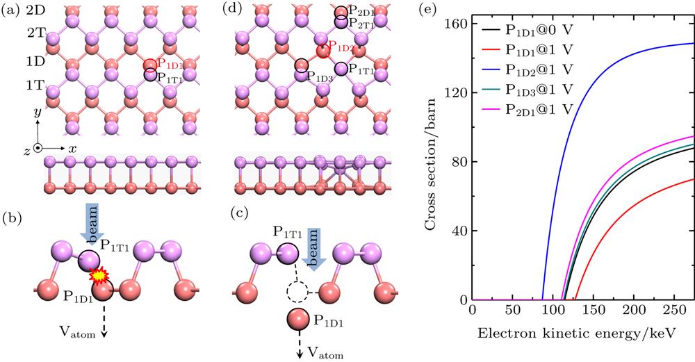
    Fig. 1. (a) Top and side views of atomic structure of monolayer BP (V0P). The names of the zigzag-like chains and two tested atoms are marked. The upper (colored in plum) and lower (colored in light coral) chains are named nT (n is the order number of the chain) and nD, respectively. The P atoms in the upper and lower sublayers are named PnTm (m is the order number of the atom) and PnDm, respectively. (b) and (c) Trajectories of two tested P atoms in pristine monolayer BP under an FHEEB. (d) Top and side views of the atomic structure of a single-atom vacancy BP (V1P) and all five tested P atoms. (e) Calculated cross-sections for the tested atoms in pristine monolayer BP (V0P) and single-atom vacancy monolayer BP (V1P).
    Atomic structures of BP with vacancies and zigzag chain vacancy. (a)–(c) Top and side views of atomic structures of BP with double-atom vacancy (V2P), triple-atom vacancy (V3P), and quadruple-atom vacancy (V4P) with the tested atoms marked on them. (d) Predicted zigzag chain vacancy in monolayer BP.
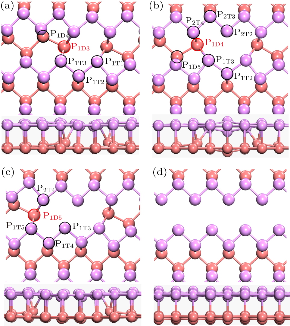
    Fig. 2. Atomic structures of BP with vacancies and zigzag chain vacancy. (a)–(c) Top and side views of atomic structures of BP with double-atom vacancy (V2P), triple-atom vacancy (V3P), and quadruple-atom vacancy (V4P) with the tested atoms marked on them. (d) Predicted zigzag chain vacancy in monolayer BP.
    Electrical properties of predicted zigzag chain vacancy in monolayer BP. (a) Band structure and density of states of the chain vacancy. (b) PCD at bands MB1 and MB2, DCD, and atomic structure of the zigzag edge chain. (c) Band structure of double-periodic chain vacancies with and without up-and-down distortion. (c) PCD at bands MB1 and MB2, DCD, and atomic structure of the zigzag edge chain. (d) Top view (left) and side view (right) of the atomic structure of the chain vacancy with distortion.
    Fig. 3. Electrical properties of predicted zigzag chain vacancy in monolayer BP. (a) Band structure and density of states of the chain vacancy. (b) PCD at bands MB1 and MB2, DCD, and atomic structure of the zigzag edge chain. (c) Band structure of double-periodic chain vacancies with and without up-and-down distortion. (c) PCD at bands MB1 and MB2, DCD, and atomic structure of the zigzag edge chain. (d) Top view (left) and side view (right) of the atomic structure of the chain vacancy with distortion.
    Five kinds of calculated edges in monolayer BP. Top views (a)–(e) and side views (f)–(j) of the atomic structures of the edges we focused on in monolayer BP. (k)–(o) Crystal directions of the corresponding edges.
    Fig. 4. Five kinds of calculated edges in monolayer BP. Top views (a)–(e) and side views (f)–(j) of the atomic structures of the edges we focused on in monolayer BP. (k)–(o) Crystal directions of the corresponding edges.
    StructureAtomsTd/eVEet/keV
    V0PP1D19.03114.8
    P1T1> 19> 225
    V1PP1T110.15127.5
    P1D26.6887.0
    P1D38.67113.4
    P2T1> 19> 225
    P2D18.55110.6
    V2PP1T112.15149.8
    P1T213.44163.7
    P1T311.06137.7
    P1D38.32106.5
    P1D49.27117.5
    V3PP1T2> 17> 201
    P1T310.79134.8
    P1D47.7599.9
    P1D58.79112.0
    P2T29.39118.9
    P2T3> 16> 191
    P2T414.49174.8
    V4PP1T39.15116.1
    P1T4> 16> 191
    P1T511.46142.2
    P1D58.44107.9
    P2T4> 14> 173
    Table 1. Displacement threshold energy and corresponding minimum electron accelerating voltage for tested P atoms in V0P and monolayer BP with V1P, V2P, V3P, and V4P.
    Yuhao Pan, Bao Lei, Jingsi Qiao, Zhixin Hu, Wu Zhou, Wei Ji. Selective linear etching of monolayer black phosphorus using electron beams[J]. Chinese Physics B, 2020, 29(8):
    Download Citation