• Photonics Research
  • Vol. 11, Issue 10, 1647 (2023)
Zihang Peng1, Yijun Huang1, Kaiyuan Zheng2, Chuantao Zheng1,*..., Mingquan Pi1, Huan Zhao1, Jialin Ji1, Yuting Min1, Lei Liang3, Fang Song1, Yu Zhang1, Yiding Wang1 and Frank K. Tittel4|Show fewer author(s)
Author Affiliations
  • 1State Key Laboratory of Integrated Optoelectronics, College of Electronic Science and Engineering, Jilin University, Changchun 130012, China
  • 2Department of Electrical Engineering and Photonics Research Institute, The Hong Kong Polytechnic University, Hong Kong 518060, China
  • 3State Key Laboratory of Luminescence and Applications, Changchun Institute of Optics, Fine Mechanics and Physics, Chinese Academy of Sciences, Changchun 130033, China
  • 4Department of Electrical and Computer Engineering, Rice University, Houston, Texas 77005, USA
  • show less
    DOI: 10.1364/PRJ.494762 Cite this Article Set citation alerts
    Zihang Peng, Yijun Huang, Kaiyuan Zheng, Chuantao Zheng, Mingquan Pi, Huan Zhao, Jialin Ji, Yuting Min, Lei Liang, Fang Song, Yu Zhang, Yiding Wang, Frank K. Tittel, "Slow-light-enhanced on-chip 1D and 2D photonic crystal waveguide gas sensing in near-IR with an ultrahigh interaction factor," Photonics Res. 11, 1647 (2023) Copy Citation Text show less
    (a) 3D schematic of the 2D PCW with a 220 nm thick Si layer and a 2 μm thick BOX layer. (b) Geometric parameters of the 2D PCW including the lattice constant a, radius of bigger air holes R, radius of center defect holes r0, waveguide width W1.1, thickness of Si h, and direction of the defect Γ−K. (c) Dispersion diagram under air and pure C2H2 background with R=0.25a and r0 =0.5R. (d) Hz distributions of even mode and odd mode when ka/2π=0.5. (e) |E| distribution of the even mode at a wavelength of 1532.83 nm. |E| distributions (f) at the cross section through a defect hole and (g) through Si slab in (e). (h) Guided mode bandwidth below the SiO2 light line in terms of wavelength (nm) and f versus r0/R ratio. (i) Simulated curves of group index and insertion loss versus the lattice constant.
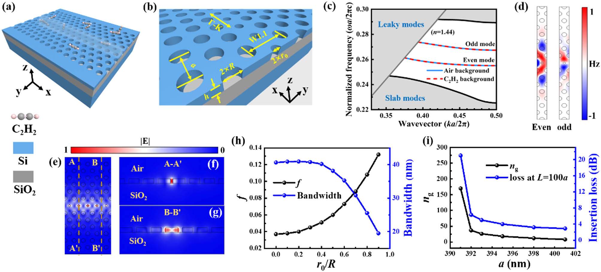
    Fig. 1. (a) 3D schematic of the 2D PCW with a 220 nm thick Si layer and a 2 μm thick BOX layer. (b) Geometric parameters of the 2D PCW including the lattice constant a, radius of bigger air holes R, radius of center defect holes r0, waveguide width W1.1, thickness of Si h, and direction of the defect ΓK. (c) Dispersion diagram under air and pure C2H2 background with R=0.25a and r0=0.5R. (d) Hz distributions of even mode and odd mode when ka/2π=0.5. (e) |E| distribution of the even mode at a wavelength of 1532.83 nm. |E| distributions (f) at the cross section through a defect hole and (g) through Si slab in (e). (h) Guided mode bandwidth below the SiO2 light line in terms of wavelength (nm) and f versus r0/R ratio. (i) Simulated curves of group index and insertion loss versus the lattice constant.
    (a) Geometric parameters of the 1D PCW including the lattice constant as, radius of air holes Rs, waveguide width w, and thickness of Si layer h. (b) Dispersion diagram under air and pure C2H2 background when Rs =0.24as and w=1.6Rs. (c) Hz distributions of the four modes in (b) at kas/2π=0.5. |E| distributions of mode 1 (d) at the horizontal section, (e) at vertical section through an air hole, and (f) through Si slab when the wavelength is 1532.83 nm. |E| distributions of mode 2 (g) at the horizontal section, (h) at vertical section through an air hole, and (i) through Si slab when the wavelength is 1532.83 nm. (j) Guided mode bandwidth and f versus w/as when Rs =0.24as, and versus Rs/as when w=1.5as. (k) Simulated curves of the group index and insertion loss versus the lattice constant as. (l) Simulated transmission of the optimized 1D PCW.
    Fig. 2. (a) Geometric parameters of the 1D PCW including the lattice constant as, radius of air holes Rs, waveguide width w, and thickness of Si layer h. (b) Dispersion diagram under air and pure C2H2 background when Rs=0.24as and w=1.6Rs. (c) Hz distributions of the four modes in (b) at kas/2π=0.5. |E| distributions of mode 1 (d) at the horizontal section, (e) at vertical section through an air hole, and (f) through Si slab when the wavelength is 1532.83 nm. |E| distributions of mode 2 (g) at the horizontal section, (h) at vertical section through an air hole, and (i) through Si slab when the wavelength is 1532.83 nm. (j) Guided mode bandwidth and f versus w/as when Rs=0.24as, and versus Rs/as when w=1.5as. (k) Simulated curves of the group index and insertion loss versus the lattice constant as. (l) Simulated transmission of the optimized 1D PCW.
    (a) 3D schematic geometric parameters of the SWG coupler including the length Lsub, width wsub, and period Psub of the air trench. (b) Equivalent model of the SWG coupler including the period of the grating and equivalent refractive index nsub. (c) Coupling efficiency to air versus period and nsub. (d) Refractive index for different fsub, calculated by EMT with zeroth-order and second-order approximations when Psub=400 nm. (e) Coupling efficiency simulated by 3D FDTD when Psub =400 nm, wsub=80 nm, period=760 nm, and Lsub=380 nm.
    Fig. 3. (a) 3D schematic geometric parameters of the SWG coupler including the length Lsub, width wsub, and period Psub of the air trench. (b) Equivalent model of the SWG coupler including the period of the grating and equivalent refractive index nsub. (c) Coupling efficiency to air versus period and nsub. (d) Refractive index for different fsub, calculated by EMT with zeroth-order and second-order approximations when Psub=400  nm. (e) Coupling efficiency simulated by 3D FDTD when Psub=400  nm, wsub=80  nm, period=760  nm, and Lsub=380  nm.
    SEM images for the fabricated (a) SWG coupler, (b) 2D PCW, (c) 1D PCW, and (d) mode transition zone in the 1D PCW.
    Fig. 4. SEM images for the fabricated (a) SWG coupler, (b) 2D PCW, (c) 1D PCW, and (d) mode transition zone in the 1D PCW.
    Measurement setup. AOM, acousto-optic modulator; PC, polarization controller; PD, photodetector; LIA, lock-in amplifier; and DAQ: data acquisition.
    Fig. 5. Measurement setup. AOM, acousto-optic modulator; PC, polarization controller; PD, photodetector; LIA, lock-in amplifier; and DAQ: data acquisition.
    (a) Measured transmitted light intensity through the 1 mm long 2D PCW when exposed to 5% C2H2. (b) Absorbance of the 2D PCW sensor versus different concentration levels of C2H2. (c) Allan deviation as a function of the averaging time τ; the insert shows the baseline stability during a 12-minute measurement test. (d) Measured transmitted light intensity through the 1 mm long 1D PCW when exposed to 5% C2H2. (e) Absorbance of the 1D PCW sensor versus different concentration levels of C2H2. (f) Allan deviation as a function of the averaging time τ.
    Fig. 6. (a) Measured transmitted light intensity through the 1 mm long 2D PCW when exposed to 5% C2H2. (b) Absorbance of the 2D PCW sensor versus different concentration levels of C2H2. (c) Allan deviation as a function of the averaging time τ; the insert shows the baseline stability during a 12-minute measurement test. (d) Measured transmitted light intensity through the 1 mm long 1D PCW when exposed to 5% C2H2. (e) Absorbance of the 1D PCW sensor versus different concentration levels of C2H2. (f) Allan deviation as a function of the averaging time τ.
    |E| distributions of the strip waveguide with a width of (a) 749 nm and (b) 610 nm at a wavelength of 1533 nm. (c) Allan deviation of the system based on IMS and DAS versus averaging time τ.
    Fig. 7. |E| distributions of the strip waveguide with a width of (a) 749 nm and (b) 610 nm at a wavelength of 1533 nm. (c) Allan deviation of the system based on IMS and DAS versus averaging time τ.
    (a) Experimental setup to measure ng. BS, beam splitter; FC, fiber coupler. Interference fringes when the lengths of the 2D PCW are 200 μm and 1000 μm, where the wavelength range is (b) 1528–1533 nm and (c) 1532.6–1533.0 nm. Interference fringes when the lengths of the 1D PCW are 200 μm and 600 μm, where the wavelength range is 1528–1536.5 nm. Curves show the group index versus the wavelength for (e) the 2D PCW and (f) the 1D PCW.
    Fig. 8. (a) Experimental setup to measure ng. BS, beam splitter; FC, fiber coupler. Interference fringes when the lengths of the 2D PCW are 200 μm and 1000 μm, where the wavelength range is (b) 1528–1533 nm and (c) 1532.6–1533.0 nm. Interference fringes when the lengths of the 1D PCW are 200 μm and 600 μm, where the wavelength range is 1528–1536.5 nm. Curves show the group index versus the wavelength for (e) the 2D PCW and (f) the 1D PCW.
    Refs.Waveguideλ (μm)L (cm)fngγSLBW (nm)α (dB/cm)LoD (ppm)
    This work2D PCW1.530.16%1146.842744277 (C2H2)
    1D PCW1.530.116%182.881010706 (C2H2)
    [19]Strip1.65100.2542772 (CH4)
    [22]Strip4.240.320.443NM (CO2)
    [12]Strip4.2610.1954NM (CO2)
    [14]Rib2.5721.076.840 (C2H2)
    [26]SWG6.652.840.243.925 (C7H8)
    [43]SWG7.3311.134.710 (acetone)
    [28]SWG6.150.310%151.54.15 (NH3)
    Table 1. Comparison of the 2D PCW, the 1D PCW, and the Reported Waveguide Gas Sensorsa
    Zihang Peng, Yijun Huang, Kaiyuan Zheng, Chuantao Zheng, Mingquan Pi, Huan Zhao, Jialin Ji, Yuting Min, Lei Liang, Fang Song, Yu Zhang, Yiding Wang, Frank K. Tittel, "Slow-light-enhanced on-chip 1D and 2D photonic crystal waveguide gas sensing in near-IR with an ultrahigh interaction factor," Photonics Res. 11, 1647 (2023)
    Download Citation