• Opto-Electronic Advances
  • Vol. 5, Issue 9, 210086 (2022)
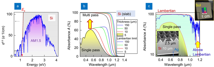
Jovan Maksimovic1、†, Jingwen Hu1、†, Soon Hock Ng, Tomas Katkus, Gediminas Seniutinas, Tatiana Pinedo Rivera, Michael Stuiber, Yoshiaki Nishijima, Sajeev John*, and Saulius Juodkazis**
Author Affiliations
  • [in Chinese]
  • show less
    DOI: 10.29026/oea.2022.210086 Cite this Article
    Jovan Maksimovic, Jingwen Hu, Soon Hock Ng, Tomas Katkus, Gediminas Seniutinas, Tatiana Pinedo Rivera, Michael Stuiber, Yoshiaki Nishijima, Sajeev John, Saulius Juodkazis. Beyond Lambertian light trapping for large-area silicon solar cells: fabrication methods[J]. Opto-Electronic Advances, 2022, 5(9): 210086 Copy Citation Text show less
    Why Si solar cells? (a) Absorption coefficient α of Si vs. photon energy (black line, grey shading) and solar spectrum profile (blue line, purple shading) at air mass AM1.5 ground conditions10. The arrow points to the bandgap energy Eg. (b) Calculated absorbance for a Si slab with different thickness in single and multiple (the Lambertian limt) passes. (c) Absorbance of 10-μm-thick Si (device layer of SOI): single pass, Lambertian limit, and calculated PhC light trapping for the used geometry6. Inset shows the PhC structure made on a Si-on-insulator (SOI) substrate which exceed the ray optics Lambertian limit6.
    Fig. 1. Why Si solar cells? (a) Absorption coefficient α of Si vs. photon energy (black line, grey shading) and solar spectrum profile (blue line, purple shading) at air mass AM1.5 ground conditions10. The arrow points to the bandgap energy Eg. (b) Calculated absorbance for a Si slab with different thickness in single and multiple (the Lambertian limt) passes. (c) Absorbance of 10-μm-thick Si (device layer of SOI): single pass, Lambertian limit, and calculated PhC light trapping for the used geometry6. Inset shows the PhC structure made on a Si-on-insulator (SOI) substrate which exceed the ray optics Lambertian limit6.
    Cr etch mask defined by direct laser writing. (a) Calibration of the ablated hole diameter D2 ∝ ln(Ep) vs. the pulse energy Ep. The threshold 0.36 nJ (0.09 J/cm2, 0.41 TW/cm2) and 5.15 nJ (1.35 J/cm2, 5.85 TW/cm2) are the intersections of dashed-lines with x-axis. The solid-line is expected evolution of D2 defined by the beam waist r = 0.61λ/NA. Top-inset shows light field E simulations for the NA = 0.9 focusing used with a Cr film on Si, for λ = 515 nm; the finite difference time domain (FDTD, Lumerical) was used. (b) SEM image of the ablated 30 nm Cr film; Ep = 1.7 nJ. The inset shows a closeup view of the ablated holes in the Cr film; the thumbnail image of the Airy pattern of the focal spot is scale matched. (c) SEM image of sample after 10 min plasma etch. The contrast change reveals the width W of the plasma etched Si (SF6:CHF3:O2 at 5:1:1 flow rate ratio). The inset shows photo of 2 × 2 cm2 area of ablated Cr mask on Si (before etch).
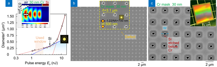
    Fig. 2. Cr etch mask defined by direct laser writing. (a) Calibration of the ablated hole diameter D2 ∝ ln(Ep) vs. the pulse energy Ep. The threshold 0.36 nJ (0.09 J/cm2, 0.41 TW/cm2) and 5.15 nJ (1.35 J/cm2, 5.85 TW/cm2) are the intersections of dashed-lines with x-axis. The solid-line is expected evolution of D2 defined by the beam waist r = 0.61λ/NA. Top-inset shows light field E simulations for the NA = 0.9 focusing used with a Cr film on Si, for λ = 515 nm; the finite difference time domain (FDTD, Lumerical) was used. (b) SEM image of the ablated 30 nm Cr film; Ep = 1.7 nJ. The inset shows a closeup view of the ablated holes in the Cr film; the thumbnail image of the Airy pattern of the focal spot is scale matched. (c) SEM image of sample after 10 min plasma etch. The contrast change reveals the width W of the plasma etched Si (SF6:CHF3:O2 at 5:1:1 flow rate ratio). The inset shows photo of 2 × 2 cm2 area of ablated Cr mask on Si (before etch).
    SEM images of a hard mask for RIE made in 50-nm-thick Cr film by laser ablation with 515 nm wavelength, 230 fs single laser pulses. Etched pattern after Cr mask removal. The inset shows an under-etch in the region where one ablation opening in the mask was absent. Conditions: NA = 0.9 lens was used, write speed 10 cm/s, pulse energy 5 nJ, laser repetition rate 200 kHz.
    Fig. 3. SEM images of a hard mask for RIE made in 50-nm-thick Cr film by laser ablation with 515 nm wavelength, 230 fs single laser pulses. Etched pattern after Cr mask removal. The inset shows an under-etch in the region where one ablation opening in the mask was absent. Conditions: NA = 0.9 lens was used, write speed 10 cm/s, pulse energy 5 nJ, laser repetition rate 200 kHz.
    (a) 10-μm-thick Si wafer cut by Ep ≈ 0.8 μJ energy fs-laser pulses (1030 nm/230 fs/200 kHz) using NA = 0.14 objective lens at 1 cm/s scan speed (5 passes with focus on the surface). SEM image of the 10-μm-thick Si wafer after cutting and patterning. Optical image of the 100-mm-diameter Si wafer on a plastic film. (b) PhC surface etched through holes ablated by fs-laser to define the Cr etch mask; NA = 0.9 lens was used, write speed 10 cm/s, pulse energy 12 nJ, laser repetition rate 200 kHz. Note the step height between regions with different period Λ. This step change is due to the under etch which is also responsible for formation of the upward-pyramid shown in inset of Fig. 3(b).
    Fig. 4. (a) 10-μm-thick Si wafer cut by Ep ≈ 0.8 μJ energy fs-laser pulses (1030 nm/230 fs/200 kHz) using NA = 0.14 objective lens at 1 cm/s scan speed (5 passes with focus on the surface). SEM image of the 10-μm-thick Si wafer after cutting and patterning. Optical image of the 100-mm-diameter Si wafer on a plastic film. (b) PhC surface etched through holes ablated by fs-laser to define the Cr etch mask; NA = 0.9 lens was used, write speed 10 cm/s, pulse energy 12 nJ, laser repetition rate 200 kHz. Note the step height between regions with different period Λ. This step change is due to the under etch which is also responsible for formation of the upward-pyramid shown in inset of Fig. 3(b).
    (a) Photo of the dot patterns (resist on Si) after exposure, development and dicing. Insets: (bottom) image of the entire 6-inch Si wafer after exposure and development; (top) the stepper reticle used for the i-line (365 nm Hg) 5× reduction (positive resist: the exposed regions are removed). (b) SEM images of 50-nm Cr film e-beam evaporated on 700-nm-thick resist patterns before and after lift-off; exposure was made by projection lithography on Si. Circular marker shows d = 200 nm for comparison with developed holes. Bottom-insets shows slanted-view images of the patterns after lift-off. Top-right inset shows the hole openings D for the four segments of PhC patterns with different periods shown in (a).
    Fig. 5. (a) Photo of the dot patterns (resist on Si) after exposure, development and dicing. Insets: (bottom) image of the entire 6-inch Si wafer after exposure and development; (top) the stepper reticle used for the i-line (365 nm Hg) 5× reduction (positive resist: the exposed regions are removed). (b) SEM images of 50-nm Cr film e-beam evaporated on 700-nm-thick resist patterns before and after lift-off; exposure was made by projection lithography on Si. Circular marker shows d = 200 nm for comparison with developed holes. Bottom-insets shows slanted-view images of the patterns after lift-off. Top-right inset shows the hole openings D for the four segments of PhC patterns with different periods shown in (a).
    (a) Photo of large 2 × 2 cm2 light trapping PhC patterns KOH etched through a chromium-mask defined by EBL; period Λ = 3.1 μm. SEM images of the final PhC pattern on 500-μm-thick n-type Si(100) wafer. (b) Color-coded presentation of portions of the absorbed A, reflected, R (measured) and transmitted T = (1 − R)10−OD (measured) light at different wavelengths from 1.67 to 25 μm (or 6000–400 cm–1 in wavenumbersν˜= 1/λ).
    Fig. 6. (a) Photo of large 2 × 2 cm2 light trapping PhC patterns KOH etched through a chromium-mask defined by EBL; period Λ = 3.1 μm. SEM images of the final PhC pattern on 500-μm-thick n-type Si(100) wafer. (b) Color-coded presentation of portions of the absorbed A, reflected, R (measured) and transmitted T = (1 − R)10−OD (measured) light at different wavelengths from 1.67 to 25 μm (or 6000–400 cm–1 in wavenumbers ν˜ = 1/λ).
    Spectral characterisation of PhC light trapping. (a) Reflectance R measured with an integrating sphere for a Si wafer, PhC on SoI (see Fig. 1(c)), and PhC defined by EBL. Note all four segments (top inset in (b)) showed the same (overlapping) spectral profile. Top inset shows (n + iκ) components27. Interference fringes of SoI sample are defined by Si thickness t = λ1λ2/[2n(λ2− λ1)] ≈ 11 μm (near-IR; n = 3.46). (b) Portions of reflected R (measured), transmitted T (measured) and absorbed A = 1 − R − T portions. Inset shows a photo of the 4-inch wafer with 4 EBL defined PhCs. (c) Reflectance of different PhC patterns prepared by laser writing and EBL which were either plasma and wet etched (note lg-axis for R). The light spot size on the sample was∼2−3 mm in diameter in order to reproduce the same conditions on samples with different areas (see the inset in (a) showing sample illuminated inside the measurement chamber).
    Fig. 7. Spectral characterisation of PhC light trapping. (a) Reflectance R measured with an integrating sphere for a Si wafer, PhC on SoI (see Fig. 1(c)), and PhC defined by EBL. Note all four segments (top inset in (b)) showed the same (overlapping) spectral profile. Top inset shows (n + iκ) components27. Interference fringes of SoI sample are defined by Si thickness t = λ1λ2/[2n(λ2λ1)] ≈ 11 μm (near-IR; n = 3.46). (b) Portions of reflected R (measured), transmitted T (measured) and absorbed A = 1 − RT portions. Inset shows a photo of the 4-inch wafer with 4 EBL defined PhCs. (c) Reflectance of different PhC patterns prepared by laser writing and EBL which were either plasma and wet etched (note lg-axis for R). The light spot size on the sample was 2−3 mm in diameter in order to reproduce the same conditions on samples with different areas (see the inset in (a) showing sample illuminated inside the measurement chamber).
    Jovan Maksimovic, Jingwen Hu, Soon Hock Ng, Tomas Katkus, Gediminas Seniutinas, Tatiana Pinedo Rivera, Michael Stuiber, Yoshiaki Nishijima, Sajeev John, Saulius Juodkazis. Beyond Lambertian light trapping for large-area silicon solar cells: fabrication methods[J]. Opto-Electronic Advances, 2022, 5(9): 210086
    Download Citation