1Key Laboratory of Luminescence and Optical Information, Ministry of Education, School of Physical Science and Engineering, Beijing Jiaotong University, Beijing 100044, China
2Hebei Key Laboratory of Optic-Electronic Information and Materials, College of Physics Science and Technology, Hebei University, Baoding 071002, China
3College of Chemistry and Life Sciences, Zhejiang Normal University, Jinhua 321004, China
Solution process is a key technique for the manufacture of large-area and low-cost semiconducting devices and, thus, attracts a lot of attention from both academia and industry. Herein, we realized solution-processed light-emitting diodes (excluding a cathode) based on aggregation-induced emission (AIE) molecules of tetraphenylethylene-4Cl (TPE-4Cl) and cadimum-free semiconductor nanocrystals (NCs) for the first time. By mixing Cu-In-Zn-S NCs and TPE-4Cl as an emissive layer, a new type of environmentally friendly white-light-emitting diodes (WLEDs) was prepared through a solution-processed technique. After systematical optimization of the as-prepared WLEDs, the corresponding color rendering index can reach up to 87 with a maximum luminance of . This study may pave a new road to realize AIE-based WLEDs through a solution-processed technique.
1. INTRODUCTION
Aggregation-induced emission (AIE) molecules have drawn tremendous attention for the importance in solid-state applications for organics since the first report in 2001 [1–10]. Especially for light-emitting devices, aggregation-caused quenching of organic dyes and luminophores was regarded as one of the main barriers in this field, while the AIE molecules successfully overcame this point and boosted the development of organic light-emitting diodes (OLEDs) [2]. Meanwhile, white OLEDs (WOLEDs) technology is one important branch of OLEDs due to their advantages of ensuring pure white emission with low cost and high efficiency [9]. Unlike monochromatic OLEDs, WOLEDs require their spectra to cover the visible region as much as possible. Therefore, multicomponent emissive layers (EMLs) are needed in most WOLEDs. In 2010, Liu et al. constructed AIE-based WOLEDs for the first time by using blue AIE molecules of TDPVBi and yellow AIE molecules of CN-DPASDB as EMLs, which demonstrated stable cold white light [Commission Internationale d'Eclairage (CIE) ] in a wide voltage range [10]. In 2018, Guo et al. realized hybrid warm WOLEDs [CIE ] by using AIE molecules TPE-TAPBI as the blue-emitting component, which provided a high power efficiency of 70.5 lm/W at . The high performance demonstrated the great potential of AIE molecules for the applications of lighting sources [8]. However, these high-performance AIE-based WOLEDs were prepared by the thermal-evaporation process, which limits the application for large-area and low-cost device manufacturing.
Recently, the solution-processed technique has been regarded as one of the most important approaches to realizing large-area and low-cost manufacturing for semiconductor devices in the industrial community because of its great compatibility with roll-to-roll and ink-printing techniques [11]. Unfortunately, all solution-processed AIE-based WOLEDs were rarely reported. On the contrary, all solution-processed techniques have achieved great success for inorganic nanocrystals- (NCs-) based WLEDs (excluding the cathode) [12–14]. Among these, Jiang et al. designed a fully solution-processed tandem white quantum-dot (QD) LED (TWQLED) based on red CdSe/ZnS QDs, green CdSe/ZnS QDs, and blue ZnCdS/ZnS QDs in 2018. This TWQLED held a high external quantum efficiency (EQE) exceeding 20% at a wide luminance ranging from 10,000 to [14]. Although the performances of these WQLEDs are high, the toxicity of heavy metals used in NCs keeps raising people’s concerns about health and environmental protection. Compared with heavy-metal-based NCs, I-III-VI-based chalcogenide semiconductor NCs attracted great interest not only for the low toxicity, earth abundance, and high luminescence efficiency, but also for the broad emission width, which will bring a higher quality of white light for binary complementary WLEDs [15,16].
In this paper, we first studied the optical properties of the hybrid layer of the AIE molecule of TPE-4Cl and bandwidth I-III-VI-based Cu-In-Zn-S (CIZS) NCs by using absorption spectroscopy, steady and transient photoluminescence (PL) spectroscopy. The results demonstrated that high-performance WLEDs can be achieved by using these two materials as EMLs. Besides, the fine compact and smooth film indicated the hybrid film has good compatibility with solution-processed WLEDs. Therefore, we constructed a new type of WLEDs with the structure of ITO/poly(3,4-ethylenedioxythiophene):poly(styrenesulfonate) (PEDOT:PSS)/poly[(9,9-dioctylfluorenyl-2,7-diyl)-alt-(4,4’-(N-(4-butylphenyl) diphenylamine)] (TFB)/EML/ZnO nanoparticles (NPs)/Al by using these hybrid layers as EMLs through a solution-processed technique. However, an unexpected deep-blue emission from the TFB layer was detected, which can be ascribed to the unbalanced charge injection and transport. To solve this problem, we introduced an additional hole transport layer (HTL) of -bis(3-methyl phenyl)--bis(phenyl)benzidine (TPD) between the poly[(9,9-dioctylfluorenyl-2,7-diyl)-alt-(-(-(4-butylphenyl) (TFB) layer and the hybrid EML to balance the charge injection. Consequently, the deep-blue emission was successfully eliminated, and high-quality white light with a color rendering index (CRI) value of 87 was obtained. By further optimization of the thickness of the double-HTL, the color of the as-prepared WLED presented outstanding stability. Although the maximum luminance of and peak EQE of 0.013% remained low and cannot be comparable with those thermal-evaporation-based WLEDs, this paper demonstrated the promising potential of the solution process in AIE-based WLEDs for the first time. We believe that this paper will pave a new road for solution-processed AIE-based optoelectronic devices.
Sign up for Photonics Research TOC. Get the latest issue of Photonics Research delivered right to you!Sign up now
2. EXPERIMENT
In the experiment, the CIZS NCs were synthesized according to our previous work [17], and the ZnO NPs were synthesized by using a solution precipitation process according to the synthetic recipe reported by Qian et al. [18].
All the devices were fabricated on indium tin-oxide- (ITO-) coated glass with a sheet resistance of about . All the ITO-coated glass was sonicated and cleaned sequentially by detergent, deionized water, acetone, and isopropanol for 15 min and repeated twice. A typical single-HTL device fabrication process is listed as follows. All the as-cleaned ITO-coated glass was treated with ultraviolet ozone for 30 min. Afterward, the PEDOT:PSS (AI 4083) was spin coated onto the ITO-coated glass at 5000 r/min and then annealed at 160°C for 30 min in air. Next, the substrates were transferred to a -filled glove box, and then TFB (8 mg/mL in chlorobenzene) was spin coated onto the PEDOT:PSS layer at 3500 r/min and annealed at 150°C for 30 min. In turn, EML with different ratios (10 mg/mL in toluene) was spin coated onto the TFB layer at 3000 r/min and annealed at room temperature for 30 min, and ZnO NPs layer (30 mg/mL in ethanol) was spin coated onto the EML at 1500 r/min and annealed at 60°C for 30 min. Finally, the Al cathode layer (100 nm) was deposited via a thermal evaporation process, and the effective area was . A typical double-layered HTL device fabrication process: the rest of the conditions remain the same as the single-HTL device, but TFB (2–8 mg/mL in chlorobenzene) was spin coated onto the PEDOT:PSS layer at 3500 r/min and annealed at 150°C for 30 min, TPD (2–8 mg/mL in -xylene) was spin coated onto the TFB layer at 3500 r/min and annealed at 90°C for 30 min.
3. RESULTS AND DISCUSSION
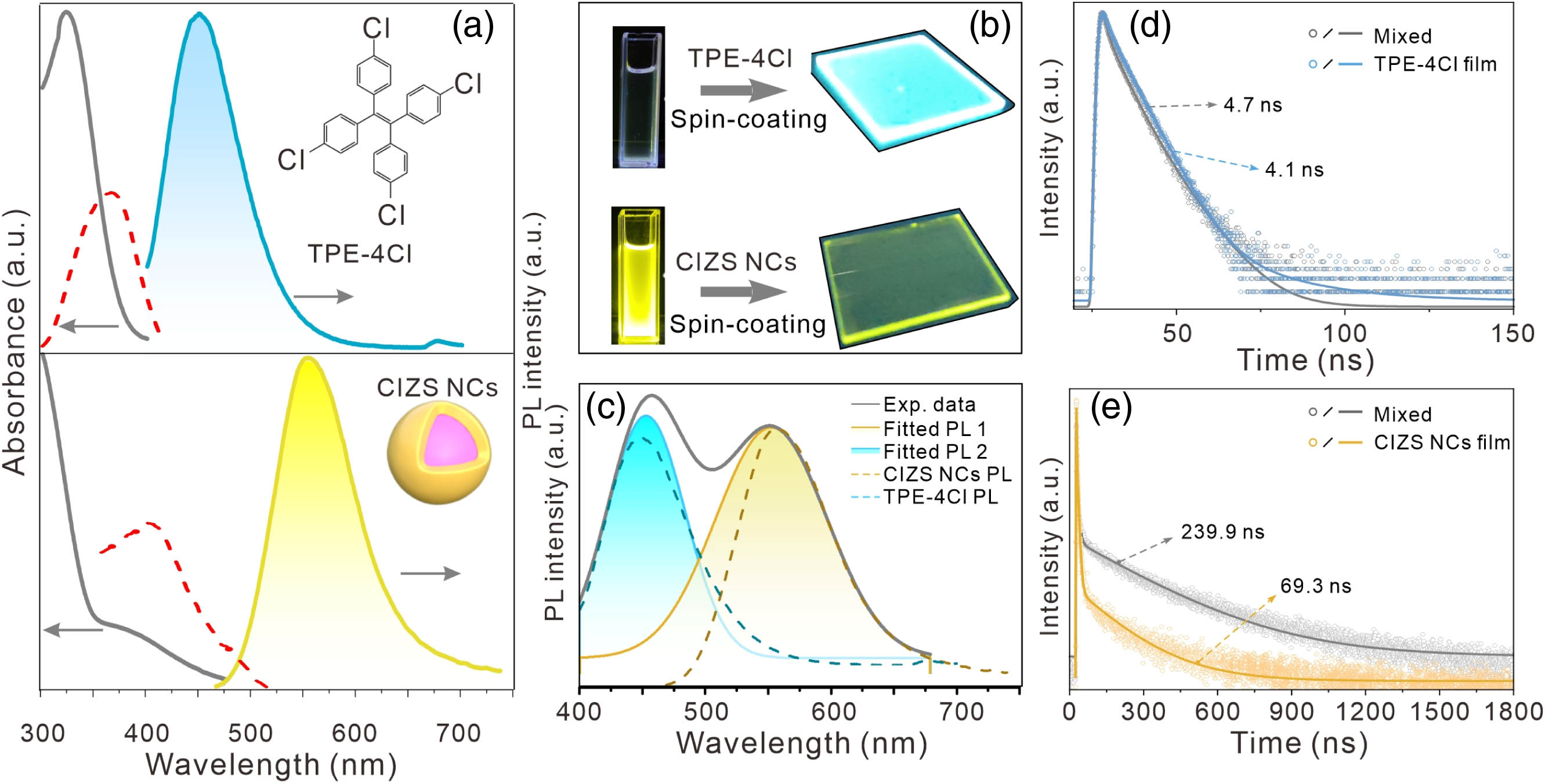
As a typical AIE material, the film of TPE-4Cl can exhibit bright blue light with a PL peak at 455 nm and a broad bandwidth of 110 nm [Figs. 1(a) and 1(b)]. The absorption spectrum of TPE-4Cl shows a sharp peak located at 327 nm, which is a characteristic peak of a TPE-based molecule and can be ascribed to the absorption of anthracene core [5,19]. The PLE [red dashed line in Fig. 1(a)] was recorded by monitoring at 455 nm, covering from 300 nm to 400 nm, which aligns with the absorption spectrum. The absorption spectrum of CIZS NCs shows a pronounced shoulder located at other than a distinguished excitonic peak [17]. The CIZS NCs film presented an emission peak of 568 nm with a broad bandwidth of [Fig. 1(b)]. Such broad spectra of both TPE-4Cl and CIZS NCs would be beneficial for improving the CRI for binary complementary WLEDs.
Figure 1.Optical properties of CIZS NCs and TPE-4Cl. (a) Absorption (Abs, gray lines) and PL spectra of CIZS film (bottom one, yellow line) and TPE-4Cl film (top one, blue line). The red dotted lines are the PL excitation (PLE) spectra of CIZS and the TPE-4Cl film; the inset shows the molecular structure of TPE-4Cl and the diagram of the CIZS NCs. (b) Photographs of TPE-4Cl and CIZS NCs in a toluene solution and films under UV light (365 nm). (c) PL spectra and corresponding fitted curves of the mixed film sample of TPE-4Cl and CIZS NCs. (d) and (e) Time-resolved PL curve and the corresponding fitted curves of TPE-4Cl and mixed film (monitored at 455 nm) as well as CIZS NCs and mixed film (monitored at 568 nm).
The PL of the mixed film was, therefore, studied. As depicted in Fig. 1(c), the broad asymmetric PL spectra can be fitted by two peaks well, which exhibited the same characteristics as TPE-4Cl and CIZS NCs. In addition, by changing the mass ratio of TPE-4Cl to CIZS NCs, the percentage of each component in PL spectra would change correspondingly, indicating the PL spectra of the hybrid film would arise from the emission of TPE-4Cl and CIZS NCs. Besides, since the existence of a partial overlap between the PL spectra of TPE-4Cl and the PLE spectra of CIZS NCs, the Förster resonant energy transfer (FRET) was expected to take place. Time-resolved PL spectra were, therefore, carried out for both two materials individually and mixed together [Figs. 1(d) and 1(e)]. The PL decay curves of both could be fitted well by a three-exponential function: where , and represent the decay time of PL emission, and , and represent the amplitude of the decay components at . The average lifetime () can be calculated by using
The fitted results can be classified as a short lifetime pathway (), a medium long lifetime pathway (), and a long lifetime pathway (). The results are summarized in Table 1. Generally, and can be ascribed to the deep defect-related nonradiative recombination and radiative recombination process, respectively, and is mainly related to the band-edge or shallow defect-related radiative recombination process [20–23]. Herein, after mixing with CIZS NCs, , and of TPE-4Cl are decreased to some extent, leading to a decrease in from 4.7 to 4.1 ns. On the other hand, CIZS NCs present an opposite trend where both pathways show a longer lifetime after mixing with TPE-4Cl, resulting in an increase in from 69.3 to 239.9 ns. This is a characteristic phenomenon of FRET and in agreement with previous works [19], which results from the transfer of excitons from TPE-4Cl to CIZS NCs. In addition, since the hybrid film can effectively enlarge the distance between CIZS NCs, the “self-quenching” results from the nonradiative FRET that occurs between interparticles can be diminished, which would make the prolong as well [24,25]. To study the morphology of the hybrid film, atomic force microscopy (AFM) was carried out. The hybrid film shows pinhole-free features, and the rms roughness is only 1.89 nm, smaller than that of the films prepared by single-CIZS NCs (2.54 nm), indicating the good dispersity of CIZS NCs in the hybrid film.
Figure 2.Color regulation and luminescence mechanism of single-TFB HTL device WLEDs. (a) Normalized EL spectra of single-TFB HTL devices based on TPE-4Cl:CIZS NCs EMLs with different ratios at 5 V. (b) EL spectra of the hybrid film (10:1), TFB film, and CIZS NCs, respectively. (c) Schematic of the EL mechanism hypothesis.
Thus, the HOMO positions of TPE-4Cl were calculated to be 5.22 eV below the vacuum level. The optical bandgaps were achieved by Tauc plots between and photon energy (). In combination with the optical bandgaps, the lowest unoccupied molecular orbital (LUMO) levels were estimated to be for TPE-4Cl.
The EL spectra of as-fabricated LEDs are shown in Fig. 3(a). A high percentage of deep-blue light was detected in electroluminescence (EL) spectra, and the deep-blue emission was hardly avoided by tuning the composition of the hybrid film. As shown in Fig. 3(b), the blue part of the emission has two peaks of 437 nm and 458 nm, which is the same as the one of the PL spectrum of TFB. Thus, it can be suspected that the deep-blue light is originated from the EL of the TFB layer. Furthermore, by comparing the EL spectra of the LEDs with the hybrid film (TPE-4Cl:), TFB, pure TPE-4Cl, and pure CIZS NCs as an active layer, we found the EL of the hybrid film can match well with the EL spectra of the combination of TFB and CIZS NCs, instead of the EL spectra of TPE-4Cl. Figure 3(c) shows the schematic of the EL mechanism hypothesis. The phenomenon can be ascribed to the unbalanced charge injection, leading to the accumulation of charge carriers on the interface of TFB and a hybrid layer, and finally some carriers can recombine in the TFB layer [27,28].
Figure 3.Schematic and cross-sectional characterization of the devices. (a) Schematic of the device structure. (b) The cross-sectional SEM image and (c) the band alignment diagram of as-fabricated devices.
To eliminate the deep-blue EL emission from TFB, an additional HTL of TPD was applied between the TFB layer and the EML. It should be noted that -xylene was selected to be the solvent for TPD to protect the TFB layer from washing damage [29]. The additional HTL can offer a deeper level of HOMO and a shallower level of LUMO, which can bring a lower-energy barrier for hole injection and a larger energy barrier for electron injection simultaneously [30–32], leading to a more balanced charge injection for the hybrid layer [Fig. 4(a)], and most of the excitons could form in the hybrid layer and give the EL emission from TPE-4Cl and CIZS synchronously [Fig. 4(b)]. Therefore, the color of the EL emission can be tuned from yellow to blue by controlling the ratio (TPE-4Cl:CIZS NCs) from 1:1 to 10:1 and by using the ratio (TPE-4Cl:CIZS NCs) of 5:1, and the nearly pure white light could be obtained [Fig. 4(b) and the inset].
Figure 4.Device performance of double-layered TFB/TPD HTLs. (a) Schematic of the carrier injection process. (b) EL spectra of the hybrid film (5:1), TPE-4Cl film, and CIZS NCs, respectively. The inset is the image of an LED under the driving voltage of 5 V. (c) Current density-voltage-luminance () curve of the device. (d) EQE and PE as a function of luminance. (e) The evolution of EL spectra with varying voltage. (f) The corresponding 1931 CIE coordinate of the EL spectra shown.
The device performance could be further improved by optimizing the thickness of the double-HTLs. The first TPD concentration was tuned from 2 mg/mL to 8 mg/mL [Figs. 5(c) and 5(d)]. Similarly, the EL spectra were barely changed as well, and the concentration of 4 mg/mL gives the best performance, which presents a low turn-on voltage of 2.4 V and a maximum luminance of [Fig. 4(c)]. The maximum EQE and power efficiency (PE) were calculated to be 0.013% and 0.014 lm/W, respectively [Fig. 4(d)]. The relatively low performance may be attributed to the negative interaction between the ligands on NCs and the TPE-4Cl molecule, resulting in the poor charge injection of NCs, which may induce more nonradiative recombination centers. Intriguingly, different from many organic–inorganic WLEDs, the plot of EQE and PE versus luminance presents a flat curve in a wide range of working windows, and the color of the as-prepared WLED exhibited outstanding stability as well as shown in Fig. 4(e). The profiles of EL spectra are nearly optimized by the thickness by varying the concentration of TFB solution from 2 mg/mL to 8 mg/mL while keeping the concentration of TPD at 4 mg/mL [Figs. 5(a) and 5(b)]. The EL spectra profiles were barely changed throughout the process, but the device with 2-mg/mL TFB showed dramatically higher leak current and turn-on voltage than the others. Subsequently, the concentration of TFB was fixed and the identical presented high CRI of 81–87 with an increase in the driving voltage from 4 V to 8 V. Accordingly, the CIE coordinates all locate in the white-light region based on the 1931 CIE diagram [Fig. 4(f)].
Figure 5.Device performance of regulation of double-HTLs: (a) EL spectra and (b) curves with different concentrations of TFB. (c) EL spectra and (d) curves with different concentrations of TPD.
To summarize, we studied the optical properties of the hybrid film (AIE molecule of TPE-4Cl and CIZS NCs), demonstrating the great potential to be the EML for WLEDs, and, therefore, the AIE-based WLEDs were fabricated through a solution-processed technique. The as-prepared LED showed an unexpected deep-blue light from the TFB layer caused by the unbalanced charge injection, which was eliminated by the introduction of additional HTL of the TPD. After systematical optimization for the double-HTL, the WLED exhibited a high and stable CRI of 87 with the CIE coordinates of (0.30, 0.33). Although the maximum luminance of and the peak EQE of 0.013% remained low in this stage, the good stability and compatibility of the solution process of these devices may lay a foundation for further study.