• Journal of Infrared and Millimeter Waves
  • Vol. 40, Issue 4, 439 (2021)
Lu-Han YANG1、2, Jia-Zhen ZHANG2, Huang XU2, Jie ZHOU2、3, Han-Xun QIU1、*, and Gang CHEN2、*
Author Affiliations
  • 1School of Materials Science and Engineering, University of Shanghai for Science and Technology, Shanghai 200093,China
  • 2State Key Laboratory of Infrared Physics, Shanghai Institute of Technical Physics, Chinese Academy of Sciences, Shanghai 200083,China
  • 3School of Mathematics and Physics, Shanghai Normal University, Shanghai 200234,China
  • show less
    DOI: 10.11972/j.issn.1001-9014.2021.04.003 Cite this Article
    Lu-Han YANG, Jia-Zhen ZHANG, Huang XU, Jie ZHOU, Han-Xun QIU, Gang CHEN. Progress in carbon nanotube films based photodetectors[J]. Journal of Infrared and Millimeter Waves, 2021, 40(4): 439 Copy Citation Text show less
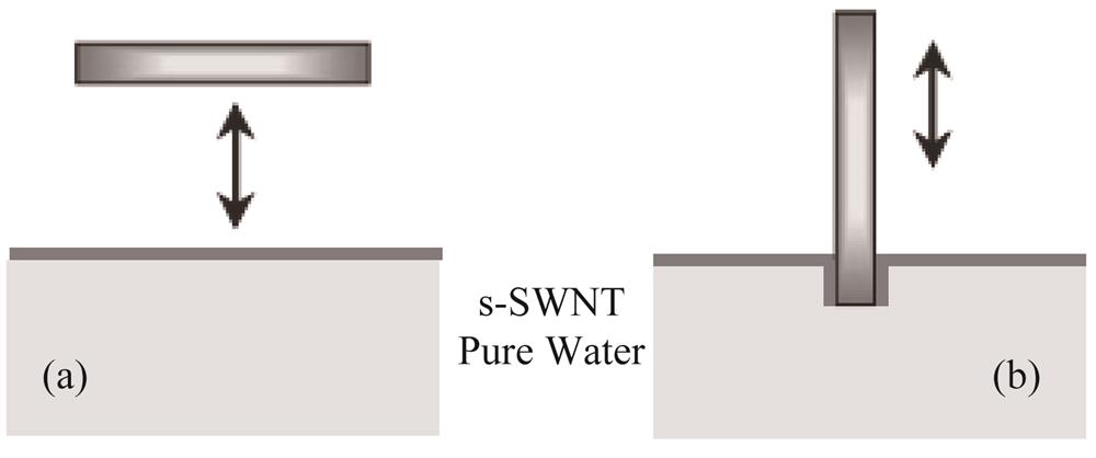
    (a)horizontal lift, (b)vertical immersion[48]
    Fig. 1. (a)horizontal lift, (b)vertical immersion48
    Schematic diagram of carbon nanotube films prepared by different angle stretching [52]
    Fig. 2. Schematic diagram of carbon nanotube films prepared by different angle stretching 52
    (a)device diagram, (b) reaction photos of hollow carbon nanotube cylinders blown from carbon nanotubes, (c)the entire carbon nanotube film removed from the substrate, (d)cut small pieces of carbon nanotube film[57]
    Fig. 3. (a)device diagram, (b) reaction photos of hollow carbon nanotube cylinders blown from carbon nanotubes, (c)the entire carbon nanotube film removed from the substrate, (d)cut small pieces of carbon nanotube film57
    (a)-(c) Macro and micro morphology of the prepared carbon nanotube film, (d) a schematic diagram of a device designed to synthesize, deposit, and transfer SWCNTS films, (e)carbon nanotube film on simple substrate[63]
    Fig. 4. (a)-(c) Macro and micro morphology of the prepared carbon nanotube film, (d) a schematic diagram of a device designed to synthesize, deposit, and transfer SWCNTS films, (e)carbon nanotube film on simple substrate63
    Fabrication and characterization of wafer-scale monodomain films of aligned CNTs (a) A CNT suspension goes through a standard vacuum filtration system. For spontaneous CNT alignment to occur, the filtration speed must be kept low and the CNTs must be well dispersed in the suspension, (b) A wafer-scale, uniform CNT film is formed on the filter membrane, (c)Optical image of the produced film after being transferred to a transparent substrate by dissolving the filter membrane, (d)a high-resolution SEM image, (e) and a top-view TEM image[76]
    Fig. 5. Fabrication and characterization of wafer-scale monodomain films of aligned CNTs (a) A CNT suspension goes through a standard vacuum filtration system. For spontaneous CNT alignment to occur, the filtration speed must be kept low and the CNTs must be well dispersed in the suspension, (b) A wafer-scale, uniform CNT film is formed on the filter membrane, (c)Optical image of the produced film after being transferred to a transparent substrate by dissolving the filter membrane, (d)a high-resolution SEM image, (e) and a top-view TEM image76
    Schematic diagram of layer by layer self-assembly of MWCNTs with negative charge[85]
    Fig. 6. Schematic diagram of layer by layer self-assembly of MWCNTs with negative charge85
    (a)-(c) Carbon nanotube optical and SEM microscopic images, (d)device preparation process and schematic diagram,(e)schematic diagram of device testing,[91]
    Fig. 7. (a)-(c) Carbon nanotube optical and SEM microscopic images, (d)device preparation process and schematic diagram,(e)schematic diagram of device testing,91
    (a)-(b) are the respective current-voltage characteristics of bolometer and PTE devices under darkness and illuminated conditions.
    Fig. 8. (a)-(b) are the respective current-voltage characteristics of bolometer and PTE devices under darkness and illuminated conditions.
    Schematics of the (a) millimeter-scale and (b) micrometer-scale CNT-based photodetector [96]
    Fig. 9. Schematics of the (a) millimeter-scale and (b) micrometer-scale CNT-based photodetector 96
    (a) suspended SWCNTs films with a thickness of 140nm, Al/Au electrode gap is 3.9mm; (b) photothermoeletric detector with p-n doping [110]
    Fig. 10. (a) suspended SWCNTs films with a thickness of 140nm, Al/Au electrode gap is 3.9mm; (b) photothermoeletric detector with p-n doping 110
    (a) The current-voltage characteristics of the photoconductive detector with or without light, (b) the current-voltage characteristics of the photodiode detector with or without light, (c) the current-voltage characteristics of the phototransistor with or without light
    Fig. 11. (a) The current-voltage characteristics of the photoconductive detector with or without light, (b) the current-voltage characteristics of the photodiode detector with or without light, (c) the current-voltage characteristics of the phototransistor with or without light
    Flexible and fully transparent photodetector based on porphyrin-SWNT-graphene heterostructure. (a)Schematic showing the fabricationof graphene electrodes, SWNT networks, and porphyrin layer on plastic substrate, (b)SEM image of boundary between graphene electrode and PET substrate after porphyrin functionalization. The SWNTs, covered by porphyrin molecules, are coated uniformly on the both graphene and PETsubstrate, (c)-(d) Photographs of as-fabricated photodetector exhibiting high transparency and flexibility[137]
    Fig. 12. Flexible and fully transparent photodetector based on porphyrin-SWNT-graphene heterostructure. (a)Schematic showing the fabricationof graphene electrodes, SWNT networks, and porphyrin layer on plastic substrate, (b)SEM image of boundary between graphene electrode and PET substrate after porphyrin functionalization. The SWNTs, covered by porphyrin molecules, are coated uniformly on the both graphene and PETsubstrate, (c)-(d) Photographs of as-fabricated photodetector exhibiting high transparency and flexibility137
    (a) Schematic diagram of graphene/s-SW CNTs cross-shaped photodiode, (b) optical image, (c) Raman spectroscopy of s-SWCNT film in radial stretching mode before and after, (d) graphene/s-SWCNT AFM image of film overlap area[138]
    Fig. 13. (a) Schematic diagram of graphene/s-SW CNTs cross-shaped photodiode, (b) optical image, (c) Raman spectroscopy of s-SWCNT film in radial stretching mode before and after, (d) graphene/s-SWCNT AFM image of film overlap area138
    (a) Schematic diagram of graphene s-SWCNTs heterostructure photocell and test circuit, (b) optical image of AS manufacturing device[151]
    Fig. 14. (a) Schematic diagram of graphene s-SWCNTs heterostructure photocell and test circuit, (b) optical image of AS manufacturing device151
    Schemes for the fabrication of the (PEA)2SnI4/semi-CNT hybrid TFTs[166]
    Fig. 15. Schemes for the fabrication of the (PEA)2SnI4/semi-CNT hybrid TFTs166
    材料响应率响应时间波长/频率
    Aligned swcnt film922.5 V/W0.11.39-3.11 THZ
    Aligned swcnt film1130.028 A/W≈32 μs0.66-3.3 μm
    Aligned swcnt film1142.5 V/W0.1 s1.39-3.11 THZ
    M-swcnt/thymine103252 V/W0.8-1.6 ms10.6 μm
    VO2/swcnts1070.017 A/W0.28 s0.8-2.5 μm
    Suspended s-swcnts960.58 A/W150 μs10 THZ
    Swcnt film95N/AN/A0.66-1.8 μm
    Aligned swcnt film115N/AN/A2.5-25 μm
    Table 1. Summary of Carbon nanotube film -based bolometric and PTE photodetectors with key device parameters from 2015to 2020
    材料响应率/(A/W)比探测率/(cmHz1/2W-1波长/μm

    S-swcnt/CO/PC71BM121

    Swcnts/SiO2132

    Swcnt film133

    Graphene/s-SWCNTfilm135

    Mwcnts/n-Si137

    Swcnts/NDIDPP134

    Swcnts/CH3NH3PbI3124

    0.25

    N/A

    N/A

    1.75

    N/A

    0.15∼0.4

    0.027~0.065

    0.9×10¹²

    N/A

    N/A

    N/A

    N/A

    2~6×10¹²

    1.2~3.8×10¹²

    0.86

    0.85∼1.2

    1.65

    0.78∼0.85

    0.6∼0.8

    0.3∼0.8

    0.4∼1.2

    Table 2. Summary of Carbon nanotube film photovoltaic detectors from 2015 to 2020
    材料响应率/(A/W)比探测率/(cmHZ1/2w-1波长/μm

    Swcnt/SGR150

    Graphene/s-SWCNT film151

    Swcnt/n-si149

    Swcnt thin film/C60153

    Swcnts/CH3NH3PbI3155

    Swcnt/SLG158

    Swcnt/graphene160

    Swcnt/PBSQDs164

    Swcnts/CH3NH3PbI3-xClx/PBSQDs165

    Swcnts/(PEA)2SnI4166

    CsBi3I10/SWNTs167

    3000

    78

    N/A

    97.5

    7.7x10⁵

    0.209

    50

    353.4

    0.5~0.35

    6.3×10⁴

    6.0×10⁴

    N/A

    N/A

    N/A

    109

    N/A

    4.8×10¹⁰

    N/A

    7.1×10¹⁰

    1.4~0.9×10¹¹

    1.12×10¹⁷

    2.46×10¹⁴

    0.38~0.77

    0.405~1.064

    0.532

    1~1.4

    0.52

    0.4~1.1

    0.4~1.2

    1.55

    0.5~1.3

    0.6~0.8

    0.74~0.76

    Table 3. Summary of Carbon nanotube film photoconductive detectors and phototransistors from 2015 to 2020
    Lu-Han YANG, Jia-Zhen ZHANG, Huang XU, Jie ZHOU, Han-Xun QIU, Gang CHEN. Progress in carbon nanotube films based photodetectors[J]. Journal of Infrared and Millimeter Waves, 2021, 40(4): 439
    Download Citation