• Advanced Photonics Nexus
  • Vol. 3, Issue 2, 026007 (2024)
Run Sun1, Tingzhao Fu2、*, Yuyao Huang1, Wencan Liu1, Zhenmin Du1, and Hongwei Chen1、*
Author Affiliations
  • 1Tsinghua University, Beijing National Research Center for Information Science and Technology, Department of Electronic Engineering, Beijing, China
  • 2National University of Defense Technology, College of Advanced Interdisciplinary Studies, Hunan Provincial Key Laboratory of Novel Nano-Optoelectronic Information Materials and Devices, Changsha, China
  • show less
    DOI: 10.1117/1.APN.3.2.026007 Cite this Article Set citation alerts
    Run Sun, Tingzhao Fu, Yuyao Huang, Wencan Liu, Zhenmin Du, Hongwei Chen. Multimode diffractive optical neural network[J]. Advanced Photonics Nexus, 2024, 3(2): 026007 Copy Citation Text show less

    Abstract

    On-chip diffractive optical neural networks (DONNs) bring the advantages of parallel processing and low energy consumption. However, an accurate representation of the optical field’s evolution in the structure cannot be provided using the previous diffraction-based analysis method. Moreover, the loss caused by the open boundaries poses challenges to applications. A multimode DONN architecture based on a more precise eigenmode analysis method is proposed. We have constructed a universal library of input, output, and metaline structures utilizing this method, and realized a multimode DONN composed of the structures from the library. On the designed multimode DONNs with only one layer of the metaline, the classification task of an Iris plants dataset is verified with an accuracy of 90% on the blind test dataset, and the performance of the one-bit binary adder task is also validated. Compared to the previous architectures, the multimode DONN exhibits a more compact design and higher energy efficiency.

    1 Introduction

    Current electronic computing devices are faced with the challenges of limited bandwidth, high power consumption, and high cost.1 These challenges promote the research enthusiasm of optical neural networks (ONNs).2,3 This is attributed to the high bandwidth and high parallelism characteristics of light, which are manifested in the ONNs composed of Mach–Zehnder interferometers (MZIs),46 micro-rings resonators (MRRs),79 scattering10 and diffraction1115 structures. It is worth noting that on-chip ONN is more competitive on portability and footprint, and even some commercial companies have been established.16 However, with the growth of data dimension or processing depth, the overheads in footprint and the number of devices of the MZI network or MRR array increase significantly and require complex correction.7,1721 Conversely, on-chip diffractive optical neural networks (DONN) exhibit remarkable integration capabilities.11,2224

    In our preceding studies, the length of the silicon (Si) etching slots in the DONNs is optimally designed to modulate the phase of the optical field carrying information, allowing classification, regression, and convolution computations to be actualized.11,2528 Notwithstanding these advancements, certain challenges have emerged. Specifically, to ensure stable interference in the DONN, a relatively large spacing between metalines and open boundaries is required, leading to severe light leakage and a substantial footprint. In addition, the previous diffraction analysis method (DAM) exhibits a decrease in accuracy as the number of metalines increases. Meanwhile, DAM is insufficient for analyzing the evolution and loss of the optical field in the output ports.

    In this paper, we propose a multimode DONN structure, in which eigenmodes are utilized as neurons. In multimode DONN, the metaline formed by Si etching slots manipulates the coupling between eigenmodes. This coupling mechanism physically realizes the connection of neurons. The corresponding eigenmode analysis method (EAM) is used to analyze the evolution of the optical field in multimode DONN, which has higher accuracy and faster calculation speed. Based on this method, a universal library including the metalines, the input and output structures are constructed. The assembled multimode DONNs complete the classification tasks of the Iris dataset and one-bit binary adder through optimization. With a smaller footprint and higher energy transfer efficiency, the multimode DONN has the potential to provide higher computing power for the next generation of artificial intelligence (AI) platforms.

    2 Structure and Principle

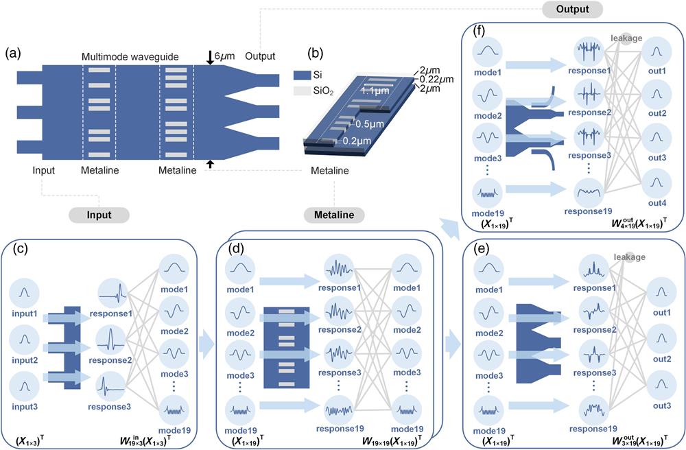
    Figure 1(a) shows the architecture of the multimode DONN. The input, output, and metaline structures are connected by the multimode waveguide, where the metaline consists of an arrangement of subwavelength units with a lateral period of 0.5  μm including the Si etching slots region and non-etching area, as shown in Fig. 1(b). The length and width of the Si etching slot are 1.1 and 0.2  μm, respectively. The input structure utilizes the width of the multimode waveguide, and several input waveguides are arranged appropriately to realize the input of the optical field modulated with information, as shown in Fig. 1(c). The optical field is guided by the multimode waveguide, then modulated by the metaline, and finally reaches the output structure. Two types of output structures are designed by multiplexing space or modes. One is a space-only multiplexing structure, where multiple inverse tapers are connected at the end of the multimode waveguide to become output waveguides, as shown in Fig. 1(e). The other is a structure that multiplexes both space and modes, such as Fig. 1(f). The inverse tapers are connected first, and then the asymmetric directional coupler is connected to construct a two-mode demultiplexer, which can guide the TE0 and TE1 modes in the bus waveguide to different output ports. The output of multimode DONN is obtained by sampling the optical power with photodetector (PD) at the output port.

    Multimode DONN and EAM. (a) Multimode DONN. As an example, the width of the multimode waveguide is 6 μm. There are 19 eigenmodes in the lateral direction. (b) The details of the metaline. The length and width of the Si etching slot are 1.1 and 0.2 μm, respectively. There are 12 positions for the Si etching slot to be placed with a lateral period of 0.5 μm, which is filled with silica. As shown in (c)–(f), the coupling between the eigenmodes physically enables the network connection. (c) Input structure. Each input fundamental mode field excites the response separately, which is decomposed into the 19 eigenmodes. (d) The 19 eigenmodes propagate independently, and the 19 responses are excited after passing through the metaline. The responses are decomposed into the 19 eigenmodes again. (e) The output structure of the multiplexing space. The 19 eigenmodes excite the 19 responses, then part of the energy in the responses is coupled to the three output waveguides, and the rest leaks out. (f) The output structure of the joint multiplexing space and mode with a total of four output ports.

    Figure 1.Multimode DONN and EAM. (a) Multimode DONN. As an example, the width of the multimode waveguide is 6  μm. There are 19 eigenmodes in the lateral direction. (b) The details of the metaline. The length and width of the Si etching slot are 1.1 and 0.2  μm, respectively. There are 12 positions for the Si etching slot to be placed with a lateral period of 0.5  μm, which is filled with silica. As shown in (c)–(f), the coupling between the eigenmodes physically enables the network connection. (c) Input structure. Each input fundamental mode field excites the response separately, which is decomposed into the 19 eigenmodes. (d) The 19 eigenmodes propagate independently, and the 19 responses are excited after passing through the metaline. The responses are decomposed into the 19 eigenmodes again. (e) The output structure of the multiplexing space. The 19 eigenmodes excite the 19 responses, then part of the energy in the responses is coupled to the three output waveguides, and the rest leaks out. (f) The output structure of the joint multiplexing space and mode with a total of four output ports.

    By analyzing the transmission and coupling of the eigenmodes, the evolution of the optical field in multimode DONN can be obtained. Therefore, the EAM is used to design and analyze multimode DONN, and the eigenmodes in multimode DONN are utilized as neurons, as will be demonstrated in the following. The multimode waveguide in Fig. 1(a) with width and thickness of 6 and 0.22  μm, respectively, is taken as an example. There are a limited number (N=19) of eigenmodes in the lateral direction. Any optical field E that can propagate stably in the waveguide can be expanded into a superposition of eigenmode optical fields En,29 and the coefficient of the superposition is an: E=n=1NanEn,an=E×Hn*·dSEn×Hn*·dS,where En and Hn represent the electric and magnetic fields of the preset n’th eigenmode, respectively. The evolution of the optical field in the multimode waveguide is the result of multimode interference. Different eigenmodes propagate independently with their propagation constant βeff[n], and the total power is P=|an|2Pn, where Pn is the power of the preset n’th eigenmode. The part of the optical field that cannot propagate stably in the multimode waveguide will appear outside Eq. (1) in the form of residuals, which will be dissipated in propagation, so the actual optical field approaches E as it propagates.

    Since the optical field response in linear materials satisfies the superposition principle, as long as obtaining the response Eresponse[n] of the metaline stimulated by n’th eigenmode, the response Eresponse of the metaline to any input E can be obtained by summing Eresponse[n] weighted an in Eq. (2). Moreover, Eresponse[n] can also be formed by weighting the eigenmodes just like Eq. (1), where the weight of m’th eigenmode is wnm. In other words, the metaline makes a coupling connection with a fixed weight wnm between the n’th eigenmode at the input and the m’th eigenmode at the output. This connection can be fully expressed by the matrix wNN of N×N dimensions. Once wNN is obtained, Eresponse can be calculated: Eresponse=n=1Nan·Eresponse[n]=n=1Nanm=1Nwnm·Em=n=1Nm=1Nwnm·an·Em.

    It should be noted that in Eq. (3), Em is only related to the multimode waveguide, and wnm is only related to the metaline. The an fully expresses the input.

    The multimode DONN serves as a mode converter,30 as shown in Figs. 1(c)1(f). The optical fields in the three input single-mode waveguides are phase- or amplitude-modulated and injected into the multimode waveguide, and the responses are decomposed into 19 eigenmodes. This process realizes the dimensionality of the input data to multiple eigenmodes. The 19 eigenmodes with information are independently propagated forward with their respective propagation coefficients. Subsequently, the Si etching slots in the metaline perturb the phase distribution of the optical field, thereby influencing the distribution of 19 eigenmodes and achieving mutual coupling among them. The output structure allows 19 eigenmodes to be coupled to the output waveguides. However, not all eigenmodes can couple losslessly to the output mode, otherwise, it would violate the reciprocity theorem.31 The mode coupling matrix of the output structure determines the proportion of each eigenmode that contributes to the output, with the remaining portion dissipating as a loss.

    Through such multimode coupling, the complex connection of the neural network is realized physically. It should be noted that eigenmodes in the multimode DONN are equivalent to neurons, instead of the slot groups11 in the previous DONN, as discussed in Sec. 4.1.

    3 Result

    Based on the EAM proposed above, a universal library consisting of the metaline, the input, and the output structures is established. The assembled multimode DONN is designed to complete the verification tasks, which include the classification task of the Iris plants dataset and one-bit binary adder.

    3.1 Build Library: Metalines, Input, and Output Structures

    The multimode waveguide with a wideness of 6  μm and thickness of 0.22  μm is still used as the basic structure. As shown in Fig. 1(b), on the lateral side of this multimode waveguide, there are 12 optional locations for placing the Si etching slot with a lateral period of 0.5  μm. Each slot can be placed or removed, resulting in a total of 212=4096 various metalines. There is a total of 19 eigenmodes in the lateral direction. The response Eresponse[n] of each metaline excited by each input eigenmode is obtained by var-FDTD simulation. Subsequently, the response is used to calculate the mode coupling matrix wNN according to Eq. (2). This matrix is recorded in the library and associated with the identification number of the metaline. The metalines in the library can be called at will to take the corresponding matrices to participate in the design and calculation. For the visualization of the mode coupling matrices, please refer to Appendix B.

    The mode coupling matrices of the input and output structures proposed in Sec. 2 are similarly obtained. For the input structure as shown in Fig. 1(c), different input ports (IN) are injected with optical fields respectively, and the responses are obtained for calculating wN×INin according to Eq. (2). It should be noted that the dimension of this matrix is the number of eigenmodes (N) multiplied by the number of IN. In the output structures as shown in Figs. 1(e) and 1(f), the response on each port after each eigenmode excitation is obtained, and then the mode coupling matrix wOUT×Nout is obtained. This is a matrix with the number of output ports (OUT) multiplied by the eigenmode number (N). If higher-order eigenmodes are considered on the output waveguide, an additional dimension, i.e., the number of eigenmodes, is required. The constructed input and output structures realize the dimensionality increase and decrease of data, and the metalines implement the complex connection.

    As shown in Fig. 2, when the task is defined, the input and output structures that fit the data dimension are picked out from the library, and they are combined with the metalines in the library to become the potential multimode DONN structures. The port-to-port transmission matrices of these potential structures can be quickly obtained by multiplying the mode coupling matrices of the separate parts, which avoids time-consuming electromagnetic simulations while maintaining high accuracy, as will be verified in Sec. 4.1. After that, the training dataset is loaded into the port-to-port transmission matrices of these potential DONN structures, and the output results will be evaluated, which may be prediction accuracy, or the desired logical result, etc. A data augmentation approach32 can be employed. Additional noise added to the training dataset14 can enhance the robustness of the multimode DONN. The best of these structures will be selected as the final multimode DONN design. In the next section, the photonic computing tasks will be validated.

    Training process and application demonstration of the multimode DONN composed of the structures in the library. When the task is defined, the training data are loaded into a variety of the potential multimode DONN structures composed of the input, output, and metalines in the library, as shown by the dotted lines. The performance of each potential multimode DONN is evaluated using the port-to-port transmission matrix and the best one is selected. Live or test data will be loaded in.

    Figure 2.Training process and application demonstration of the multimode DONN composed of the structures in the library. When the task is defined, the training data are loaded into a variety of the potential multimode DONN structures composed of the input, output, and metalines in the library, as shown by the dotted lines. The performance of each potential multimode DONN is evaluated using the port-to-port transmission matrix and the best one is selected. Live or test data will be loaded in.

    3.2 Iris Classification

    To complete the Iris classification task, the input structure with four ports satisfying the input data dimension and the output structure with three ports satisfying the classification categories are first selected from the library. Cooperating with the metalines in the library, the assembled multimode DONN is used to complete the task, as shown in Fig. 3(a) (more details in Appendix A). Three kinds of Iris are classified according to the length and width of the calyx and petals. These data are normalized and mapped to 0π, which are phase modulated to the fundamental mode field of the input waveguides. This optical field is fed into the multimode DONN and passes through the metaline. The category corresponding to the output port receiving the highest power is judged as a classification result.

    The classification task of the Iris plants dataset. (a) Multimode DONN structure. The category corresponding to the output port receiving the highest power is judged as a classification result. PD, photodetector. (b) A set of Setosa class data is simulated by var-FDTD. (c) The confusion matrix of the test dataset. (d) Fundamental mode amplitudes for the three output ports of the test dataset. The gray and yellow bars mark the dataset presented in (b) and the three misclassified datasets, respectively.

    Figure 3.The classification task of the Iris plants dataset. (a) Multimode DONN structure. The category corresponding to the output port receiving the highest power is judged as a classification result. PD, photodetector. (b) A set of Setosa class data is simulated by var-FDTD. (c) The confusion matrix of the test dataset. (d) Fundamental mode amplitudes for the three output ports of the test dataset. The gray and yellow bars mark the dataset presented in (b) and the three misclassified datasets, respectively.

    To train the multimode DONN for the Iris classification task, the training methodology in Sec. 3.1 is employed. The training dataset is loaded into the port-to-port linear transformation matrices of the potential multimode DONN, which is obtained by multiplying the mode coupling matrices of the separate parts in the library. The intensity of each output port is calculated, and the accuracy of the classification results of the different potential multimode DONNs is recorded. The metaline numbered as 1438 in the library has the highest accuracy and is selected as the preferred structure. The test dataset is identically loaded into the multimode DONN with the selected metaline, and the accuracy of the blind test dataset is 90%. The confusion matrix of the test dataset is shown in Fig. 3(c), and the fundamental mode amplitudes of the three output ports for the test dataset are shown in Fig. 3(d). Var-FDTD has conducted simulation verification of the device, as shown in Fig. 3(b), which has a correct classification result and shows the same accuracy rate on the Iris test dataset. Figure 3(d) also shows the power of output. Compared with the previous works,11,25,28 the energy efficiency has been significantly improved. It means a higher tolerance for detection noise. The computing part of the whole device occupies about 6  μm×15  μm, which has the characteristics of high integration.

    3.3 One-Bit Binary Adder

    Similarly based on the library, a three-input structure that multiplexes space, a metaline, and a four-output structure that multiplexes space and mode, are assembled to complete a one-bit binary adder, as shown in Fig. 4(a) (more details in Appendix A). The four input cases in the truth table and a constant reference bias are modulated to the phase of the input optical field, as shown in Table 1. 0 (1) corresponds to 0 (π), and the reference bias phase continues to be 1, i.e., π. The power of the symmetrical upper and lower ports is detected and compared. If the power of the upper (lower) port is higher, the output is 1 (0). Similar to the training methodology in Sec. 3.1, the metaline number 347 is selected because of the higher contrast between the upper and lower ports. Figure 4(b) shows var-FDTD simulation results for four input cases. Moreover, the power of each output port is shown in Fig. 4(c) on the right.

    One-bit binary adder. (a) Multimode DONN and discriminant structure. (b) Var-FDTD simulation of four input cases. (c) The power of the four output ports normalized to the input port power. Ports 1 to 4 indicate the marked ports, as shown by the dashed gray lines.

    Figure 4.One-bit binary adder. (a) Multimode DONN and discriminant structure. (b) Var-FDTD simulation of four input cases. (c) The power of the four output ports normalized to the input port power. Ports 1 to 4 indicate the marked ports, as shown by the dashed gray lines.

    InputBIASOutput
    IN-1IN-2OUT-1OUT-2
    00100
    01101
    10101
    11110

    Table 1. The truth table of a one-bit binary adder.

    4 Discussion

    4.1 Comparison of the Multimode DONN with the Previous DONNs

    There are three structural differences between the previous DONNs based on DAM and the multimode DONNs. In the previous DONNs, first, metalines are arranged in a Si slab with lateral-open borders, as shown in Fig. 5(a). The lack of borders is to reduce reflection, but the energy leaking out is not utilized. Second, multiple14,25 (2, normally) identical Si etching slots in metaline need to be clustered together to form a quasi-periodic medium structure group, which occupies multiple lateral periods of the slot, so that the previous DONNs become very wide. Third, the spacing between adjacent metalines needs to be much greater than the lateral period of the slot, otherwise far-field stable interference cannot be formed and the phase shift created by the structure groups, as shown in Fig. 5(b), will also change due to excessive inclination angle,14,25 which will seriously affect the accuracy of the DAM. All of the above problems arise to meet the preconditions of DAM, which significantly limits the integration capability and the optical energy efficiency of the previous DONNs. As long as the multimode DONN no longer relies on the DAM, these problems can be avoided.

    Previous DONN layout. (a) Every three identical Si etching slots form a group in the metaline, which is laid in a lateral open Si slab. wpq represents the diffractive connection between the points p and q, which are placed in the adjacent metalines. (b) Phase shift or transmittance versus the length of the group, except for the length of the group, and the parameters of the Si etching slot are consistent with Fig. 1(b) (more details in Appendix A).

    Figure 5.Previous DONN layout. (a) Every three identical Si etching slots form a group in the metaline, which is laid in a lateral open Si slab. wpq represents the diffractive connection between the points p and q, which are placed in the adjacent metalines. (b) Phase shift or transmittance versus the length of the group, except for the length of the group, and the parameters of the Si etching slot are consistent with Fig. 1(b) (more details in Appendix A).

    To demonstrate the advantages of EAM over DAM in terms of accuracy and computational overhead, the following structures are designed. Identical metalines are cascaded and deployed respectively in the same position of the lateral-open Si slab and the multimode waveguide with a transverse width of 20  μm, such as that shown in Figs. 6(a) and 6(c). The spacing from the input facet to the first metaline and from the first metaline to the second is 40  μm, which fits the length limit of the DAM as much as possible (more details in Appendix A). Ten groups of Si etching slots are deployed in each metaline, and the length of the groups is randomly set at 0 to 2.2  μm so that the phase modulation of each group can cover the entire 2π, as shown in Fig. 5(b). The input waveguides are loaded with optical fields with random amplitude and phase. The discrepancy between the normalized optical fields E^ and E, obtained by DAM (EAM) and var-FDTD simulation, respectively, is measured by root mean square error (RMSE): RMSE=1PP(|E^||E|)2,where P=1122 is the number of sampling points. As shown by the blue line in Fig. 6(b), the downward trend represents a gradual improvement of the accuracy in DAM as the propagation length increases. This confirms the problem that the spacing between the adjacent metalines cannot be too short. The RMSE rises sharply after each metaline, and the RMSE at the end has reached 0.124, which is 4.6 times that of the input (0.027). The difference between the optical field calculated by the DAM and var-FDTD is obvious, as shown in Figs. 6(e) and 6(f). However, the RMSE of the EAM grows slowly, as shown by the green line in Fig. 6(b). Therefore, the spacing does not significantly affect the accuracy of EAM. After passing through the metalines, the RMSE does not rise evidently, and RMSE=0.049 at the output is 1.63 times that of RMSE=0.03 at the input. As shown in Figs. 6(g)6(i), in front of the metalines or at the end, compared with the DAM, the field obtained by the EAM has a higher fitting accuracy with var-FDTD. In the process of constructing Fig. 6(b), the DAM takes 7400 s, which is about 104 times longer than the EAM takes 71 s. This demonstrates that the EAM has less computational overhead. A personal desktop computer was utilized for simulation and computation.

    The optical fields calculated by the DAM and EAM are compared. (a) The amplitude of the optical field in the lateral open device obtained by var-FDTD. (b) RMSE of DAM or EAM varies with the propagation distance. The gray narrow strip areas are the metalines. (c) The amplitude of the optical field in the multimode device is obtained by var-FDTD simulation. (d)–(i) Comparison of the optical fields calculated by the DAM (EAM) or var-FDTD in front of the first and second metalines, and at the end.

    Figure 6.The optical fields calculated by the DAM and EAM are compared. (a) The amplitude of the optical field in the lateral open device obtained by var-FDTD. (b) RMSE of DAM or EAM varies with the propagation distance. The gray narrow strip areas are the metalines. (c) The amplitude of the optical field in the multimode device is obtained by var-FDTD simulation. (d)–(i) Comparison of the optical fields calculated by the DAM (EAM) or var-FDTD in front of the first and second metalines, and at the end.

    The characteristic of multimode DONN to save optical energy is also reflected. The ratio of the optical power obtained at the end cross-section of the structure is defined as the energy transfer efficiency (T). The structure with the multimode waveguide reflects the light that leaks from the open boundary in the previous structure, thereby increasing the energy transfer efficiency from T=0.68 in previous structure to T=0.95. The remaining loss comes from the dissipation in the transmission process. As the number of metalines increases, the difference in T becomes more obvious. Higher transmission efficiency means smaller input energy requirement and lower detection sensitivity, which is beneficial to reducing computing power consumption.

    By comparison, EAM demonstrates higher analysis and design accuracy with less computational overhead. This significant advantage over DAM promotes the design of multimode DONN, achieving both high precision and speed. The formation of the multimode DONNs’ boundaries is attributed to the eigenmodes that serve as the foundation for analysis. This enhances energy transfer efficiency while allowing for a further reduction in the footprint of the multimode DONN to increase integration density. The following section will provide evidence for this.

    4.2 Footprint and Optical Loss

    It is beneficial to reduce the footprint by making full use of the multimode. In the ONN implemented by the MZI network,46 a single waveguide has only one eigenmode, and the coupling between adjacent eigenmodes is accomplished by a directional coupler.17 The distance between the arms is generally maintained at more than a few microns to ensure that no crosstalk occurs. Potential multimode in this space is not utilized as much as possible. To realize the coupling between each single mode, a multilayer directional coupler array4,5,18,19 is necessary; however, this coupling connection between the modes can be completed by a metaline. The previous DONN is designed based on the DAM. Since the single neuron must be mapped by the Si etching slot group, the lateral period of the neurons is about 1.5  μm,11 while the lateral density in multimode DONN is about 315 nm per neuron (mode), and the EAM ensures that the multimode DONN no longer requires large metaline spacing. As a result, the footprint of the multimode DONN in this work is at least nine times smaller than that of previous identical or similar tasks (classification or convolution). The comparison results are shown in Table 2.

    WorksDesign methodFootprint (μm2)Number of input × outputTypical loss (dB)
    Ref. 11DAM1000×2804×3−14.55
    Ref. 28DAM1200×759×2−22.01
    Ref. 33DAM and fitting network30×504×3−8.86
    Ref. 27Particle swarm search45×304×3−13.01
    This workEAM and library15×104×3−7.69

    Table 2. Comparison with previous works.

    The optical loss introduced by the multimode DONN as a passive device is considered. Taking the total optical energy injected into the device as the reference value, the maximum optical power at the output port is utilized to calculate the typical optical loss. However, the previous works11,27,28,33 overlooked the output structures, allowing for comparison solely based on the optical power at the output cross-section, and the typical losses based on var-FDTD simulation are presented in the last column of Table 2. In Fig. 3(b), the typical loss for the multimode DONN in performing the Iris classification task is below 7.69 dB, which is lower compared to the previous works. When considering the loss caused by the output structures of other works, this difference becomes even more pronounced. Hence, the multimode DONN exhibits energy-saving characteristics.

    4.3 Metalines and I/O Structure

    The metaline is the core structure for computation in the multimode DONN, selected from the library by EAM. In this work, the task-agnostic library comprises 4096 metalines constructed by exploring the presence or absence of etching slots. As the etching slots in metaline share the same design, the consistent errors manifested during fabrication can be incorporated into the structure during library construction. This helps mitigate the impact of fabrication errors. The computation of the mode coupling matrices for the metalines in the library was completed using three server-grade computers over about 60 h. When two metalines are symmetric, their mode coupling matrices have the following relationship: wnm={wnmsymmetry(n+m)is evenwnmsymmetry(n+m)is odd.This allows for the calculation of some metalines to be omitted, aiming to save time. Phase-change materials34,35 can fill the Si etching slots, and its two steady states of the refractive index correspond to the presence or absence of the etching slots. Cascading metalines contribute to improving the computational performance of the multimode DONN since it enhances the diversity of the mode coupling matrices. For instance, the accuracy of the Iris classification task in the multimode DONN cascading two metalines can be further improved to 93.3% (more details can be found in Appendix A).

    The structures that multiplex space or modes are adopted as input-output configurations in this work. Many new compact and stable mode or meta-structure device36,37 can be included in the library when their mode coupling matrices are obtained. In this work, data are loaded into the multimode DONN by phase modulation, as metalines manipulate the phase of the optical field, and the input power is stable. In addition, phase modulators are simple and mature.

    4.4 Scalability of the Multimode DONNs

    With the aim of enhancing the data processing capability of the multimode DONN, the following approaches can be considered. First, higher-order eigenmodes in the multimode DONN can be multiplexed to expand input-output capacity, requiring additional higher-order mode multiplexers and demultiplexers.38 Furthermore, by deploying multiple multimode DONNs in a distributed and layered manner,39 the data processing capacity of the multimode DONN can be further increased, allowing optical fields to interact across multiple multimode DONNs.

    Library-based EAM can be combined with other differential optimization methods. The multimode DONN designed based on the library can serve as a seed structure for optimization using particle swarm optimization27 or the adjoint field method.40 In addition, utilizing EAM can bypass the positions where structures are not allowed to be deployed and input-output structures, enhancing the calculation speed of the optical field.

    Built upon the foundation of multimode waveguides, the multimode DONN is compatible with integration into multimode systems,41 achieving an integrated solution for transmission and processing. Optoelectronic hybrid networks have emerged as a new application paradigm.15 The multimode DONN can perform feature extraction and processing of data, while electronic neural networks carry out further computations on the data. The electronic neural network enhances the flexibility of the hybrid network28 and can correct system errors42 to adapt to more complex tasks.

    5 Conclusion

    In this paper, we introduce a compact multimode DONN structure, where eigenmodes are employed as neurons. Simultaneously, leveraging the proposed EAM, a universal library of structures, including metalines, input, and output structures, is established. Each structure is characterized by a mode coupling matrix. Through optimization, the most suitable structures are selected to compose the multimode DONN for validation tasks, including the Iris classification and one-bit binary adder. For similar or identical tasks, the multimode DONN exhibits a smaller footprint and consumes less optical power budget. It implies that the multimode DONN has higher integration density and scalability capability. Benefiting from the good compatibility and precise optical field representation capability of the EAM, the designed multimode DONN offers a new solution for compact and parameterized ONNs.

    6 Appendix A: Structure and Simulation Details

    The parameters of the structure shown in Fig. 3(a) are as follows. The widths of the input and output waveguides are both 450 nm, with spacings of 1.5 and 2  μm, respectively. The distance from the front of the multimode waveguide to the metaline is 3.2  μm, while the distance between the metaline and the output taper is 1.9  μm. The length of the taper is 8  μm.

    The parameters of the structure shown in Fig. 4(a) are as follows. The widths of the input and output waveguides are both 450 nm. The spacing between input waveguides is 2.775  μm. The distance from the front of the multimode waveguide to the metaline is 5.7  μm, while the distance between the metaline and the output taper is 2  μm. The output structure comprises two symmetrical two-mode demultiplexers. The first taper has a length of 31  μm, with a width gradually varying from 3  μm to 966 nm. The coupling region’s length is 22.6  μm with a spacing of 200 nm. The second taper has a length of 17.3  μm, with a width gradually varying from 960 to 450 nm.

    The parameters of the structure shown in Fig. 5(b) are as follows. Si etching slots consistent with Fig. 1(b) are arranged periodically at a 500 nm pitch. The length varies within the range of 0 to 2.2  μm. Sampling points are set at 100 nm before and 2.3  μm after the center point of the front surface of the slot to observe phase variations. The difference between the observed phase change and the background phase without etching is documented.

    The spacing of the input waveguides in Figs. 6(a) and 6(c) is 1  μm, with a width of 450 nm.

    The multimode DONN with two layers of metalines is employed to accomplish the Iris classification task. In comparison to the structure depicted in Fig. 3(a) of Sec. 3.2, the second layer of metalines is positioned 2.5  μm behind the first layer. Following a multimode waveguide with a length of 1.05  μm, the same output structure is cascaded. The combined structure of metaline 2750 and metaline 748 is chosen.

    The var-FDTD grid within the metaline region has dimensions of 8, 5, and 14.2 nm in the x, y, and z directions, respectively.

    7 Appendix B: Visualization of the Mode Coupling Matrices for the Metalines in the Library

    In Sec. 3.1, the 4096 metalines in the library are grouped based on the number of Si etching slots. As shown in Fig. 7, the quantity of metalines in each group is listed above the images. The average amplitude of the mode coupling matrix elements for each group of metalines is presented in the top images. The bottom images depict the variance. With an increasing number of etching slots, the mode coupling matrices gradually diverge from the identity matrix, and the variance initially increases and then decreases.

    Average and variance of mode coupling matrices categorized by the number of Si etching slots. The 4096 metalines obtained in Sec. 3.1 of the main text are classified based on the number of etching slots, ranging from 0 to 12. The quantity of the metalines in each group is listed above the images. The top image in each group displays the average amplitude of the elements in the mode coupling matrices, while the bottom image shows the variance. The numbers in the horizontal direction are the input mode numbers, and the numbers in the vertical direction are the output mode numbers.

    Figure 7.Average and variance of mode coupling matrices categorized by the number of Si etching slots. The 4096 metalines obtained in Sec. 3.1 of the main text are classified based on the number of etching slots, ranging from 0 to 12. The quantity of the metalines in each group is listed above the images. The top image in each group displays the average amplitude of the elements in the mode coupling matrices, while the bottom image shows the variance. The numbers in the horizontal direction are the input mode numbers, and the numbers in the vertical direction are the output mode numbers.

    Biographies of the authors are not available.

    References

    [1] H. N. Khan, D. A. Hounshell, E. R. H. Fuchs. Science and research policy at the end of Moore’s law. Nat. Electron., 1, 14-21(2018).

    [2] Y. Bai et al. Photonic multiplexing techniques for neuromorphic computing. Nanophotonics, 12, 795-817(2023).

    [3] P. Freire et al. Artificial neural networks for photonic applications-from algorithms to implementation: tutorial. Adv. Opt. Photonics, 15, 739-834(2023).

    [4] S. Pai et al. Experimental evaluation of digitally verifiable photonic computing for blockchain and cryptocurrency. Optica, 10, 552-560(2023).

    [5] Y. Shen et al. Deep learning with coherent nanophotonic circuits. Nat. Photonics, 11, 441-446(2017).

    [6] I. A. D. Williamson et al. Reprogrammable electro-optic nonlinear activation functions for optical neural networks. IEEE J. Sel. Top. Quantum Electron., 26, 7700412(2020).

    [7] B. Bai et al. Microcomb-based integrated photonic processing unit. Nat. Commun., 14, 66(2023).

    [8] J. Cheng et al. Human emotion recognition with a microcomb-enabled integrated optical neural network. Nanophotonics, 12, 3883-3894(2023).

    [9] W. Zhang et al. Broadband physical layer cognitive radio with an integrated photonic processor for blind source separation. Nat. Commun., 14, 1107(2023).

    [10] E. Khoram et al. Nanophotonic media for artificial neural inference. Photonics Res., 7, 823-827(2019).

    [11] T. Fu et al. Photonic machine learning with on-chip diffractive optics. Nat. Commun., 14, 70(2023).

    [12] X. Lin et al. All-optical machine learning using diffractive deep neural networks. Science, 361, 1004-1008(2018).

    [13] C. Qian et al. Performing optical logic operations by a diffractive neural network. Light Sci. Appl., 9, 59(2020).

    [14] Z. Wang et al. Integrated photonic metasystem for image classifications at telecommunication wavelength. Nat. Commun., 13, 2131(2022).

    [15] Y. Chen et al. All-analog photoelectronic chip for high-speed vision tasks. Nature, 623, 48-57(2023).

    [16] E. Cartlidge. Photonic computing for sale. Opt. Photonics News, 34, 26-33(2023).

    [17] W. R. Clements et al. Optimal design for universal multiport interferometers. Optica, 3, 1460-1465(2016).

    [18] Y. Huang et al. Easily scalable photonic tensor core based on tunable units with single internal phase shifters. Laser Photonics Rev., 17, 2300001(2023).

    [19] S. Pai et al. Experimentally realized in situ backpropagation for deep learning in photonic neural networks. Science, 380, 398-404(2023).

    [20] W. Zhang et al. Silicon microring synapses enable photonic deep learning beyond 9-bit precision. Optica, 9, 579-584(2022).

    [21] W. Zhang et al. On-chip photonic spatial-temporal descrambler. Chip, 2, 100043(2023).

    [22] Z. Wang et al. Metasurface on integrated photonic platform: from mode converters to machine learning. Nanophotonics, 11, 3531-3546(2022).

    [23] Z. Wu et al. Neuromorphic metasurface. Photonics Res., 8, 46-50(2019).

    [24] H. H. Zhu et al. Space-efficient optical computing with an integrated chip diffractive neural network. Nat. Commun., 13, 1044(2022).

    [25] T. Fu et al. On-chip photonic diffractive optical neural network based on a spatial domain electromagnetic propagation model. Opt. Express, 29, 31924-31940(2021).

    [26] T. Fu et al. Integrated diffractive optical neural network with space-time interleaving. Chin. Opt. Lett., 21, 091301(2023).

    [27] T. Fu et al. Miniature on-chip diffractive optical neural network design, JW2A.135(2023).

    [28] Y. Huang et al. Sophisticated deep learning with on-chip optical diffractive tensor processing. Photonics Res., 11, 1125(2023).

    [29] A. W. Snyder, A. W. Snyder. Optical Waveguide Theory(1983).

    [30] D. A. B. Miller. All linear optical devices are mode converters. Opt. Express, 20, 23985-23993(2012).

    [31] D. Jalas et al. What is-and what is not-an optical isolator. Nat. Photonics, 7, 579-582(2013).

    [32] B. Li, Y. Hou, W. Che. Data augmentation approaches in natural language processing: a survey. AI Open, 3, 71-90(2022).

    [33] W. Liu et al. C-DONN: compact diffractive optical neural network with deep learning regression. Opt. Express, 31, 22127-22143(2023).

    [34] J. Feldmann et al. Parallel convolutional processing using an integrated photonic tensor core. Nature, 589, 52-58(2021).

    [35] C. Wu et al. Programmable phase-change metasurfaces on waveguides for multimode photonic convolutional neural network. Nat. Commun., 12, 96(2021).

    [36] Y. Liu et al. Arbitrarily routed mode-division multiplexed photonic circuits for dense integration. Nat. Commun., 10, 3263(2019).

    [37] Y. Meng et al. Optical meta-waveguides for integrated photonics and beyond. Light Sci. Appl., 10, 235(2021).

    [38] D. Dai et al. 10-channel mode (de)multiplexer with dual polarizations. Laser Photonics Rev., 12, 1700109(2018).

    [39] M. E. Marhic. Hierarchic and combinatorial star couplers. Opt. Lett., 9, 368-370(1984).

    [40] T. W. Hughes et al. Adjoint method and inverse design for nonlinear nanophotonic devices. ACS Photonics, 5, 4781-4787(2018).

    [41] C. Li, D. Liu, D. Dai. Multimode silicon photonics. Nanophotonics, 8, 227-247(2019).

    [42] Z. Zheng et al. Dual adaptive training of photonic neural networks. Nat. Mach. Intell., 5, 1119-1129(2023).

    Run Sun, Tingzhao Fu, Yuyao Huang, Wencan Liu, Zhenmin Du, Hongwei Chen. Multimode diffractive optical neural network[J]. Advanced Photonics Nexus, 2024, 3(2): 026007
    Download Citation