
Jing Ma, Dongdong Liu, Jicheng Wang, Zhengda Hu. Plasmonic sensor with variable claddings based on metallic slit arrays[J]. Chinese Optics Letters, 2018, 16(3): 032301
- Chinese Optics Letters
- Vol. 16, Issue 3, 032301 (2018)
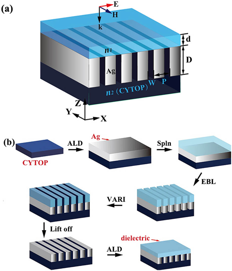
Fig. 1. (a) Schematic of the proposed metallic nanoslit arrays with a top variable dielectric and a CYTOP substrate. (b) Schematic of the fabrication process for the proposed structure.
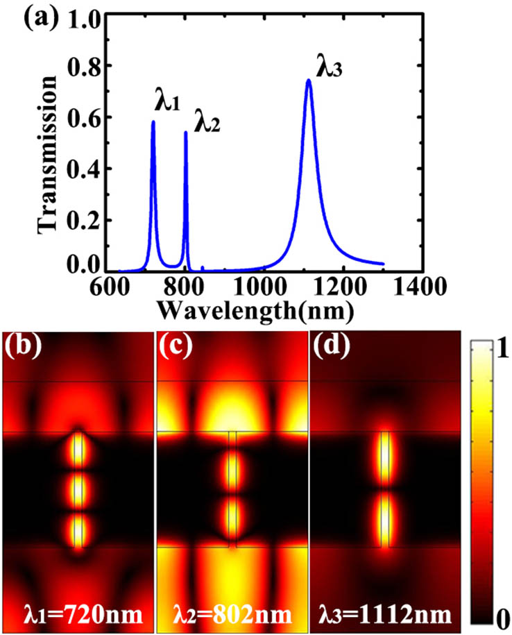
Fig. 2. (a) Transmission spectrum of the top-layer silica with normal incidence. Magnetic field distributions of the device region at (b) CM 2 CM 1
Fig. 3. Comparison of the transmission spectra of (a) different top materials and (b) gain-assisted materials (the inset provides a clear picture of the peak position).
Fig. 4. Transmission spectra for incident angles from 5° to 30°. Different color lines denote distinct incident angles. The inset figure shows the schematic structure of the oblique incidence with variable incident angle α
Fig. 5. (a) Transmission spectra of the first-order CM of the periodic metal structure with different values of period. (b) Transmission intensities as a function of the corresponding wavelength (λ 3
Fig. 6. Simulated transmission spectra of the designed structure with P = 600 nm D = 460 nm
Fig. 7. (a) Transmission intensity as a function of wavelength (λ 3 CM 1 P = 600 nm W = 30 nm d = 200 nm

Set citation alerts for the article
Please enter your email address
© Copyright 2018-2021 | Chinese Laser Press. All Rights Reserved 沪ICP备15018463号-20