We propose a plasmonic sensor with variable refractive index (RI), which exhibits high sensitivity and extraordinary optical transmission (EOT). Its variable RI is attributed to its dielectric layers and metallic slit arrays. According to simulation results, the third resonant wavelength has a wavelength sensitivity of 800 nm/RIU and an ultra-high transmittance of 0.8 by adjusting the RIs of the upper and lower dielectrics, incident light angle, and structural geometric parameters. With its unique features, the proposed structure holds considerable potential for extensive application to metal–dielectric grating sensors operating at visible and near-infrared frequencies.
Based on the excitation of coupled surface plasmon polaritons (SPPs)[1,2] on the top and bottom interfaces of a two-dimensional (2D) dielectric–metal–dielectric grating structure, real-time and label-free sensing called surface plasmon resonance (SPR) sensing[3] is the most rapidly advancing research area in nano-optics. Therefore, the SPR sensing, which can be considered as the plasmonic sensor, has come into view as a significant technology because of the excellent characteristics about ultra-high sensitivity and extraordinary optical transmission (EOT)[1,4]. The applications and devices based on a one-dimensional (1D) grating have been investigated extensively, and a great progress has been made in biology[5], medicine[6], energy[7], and optics[8–10].
The transmission spectra of metal plasmonic nanostructures are sensitive to the change in the environmental refractive index (RI) around nano-arrays and geometric parameters. Thus, SPP-EOT-based metal nano-array sensors have been investigated substantially in previous scientific studies[11–16]. Wavelength sensitivity () and figure of merit () are used to evaluate the capability of a sensor. Here, is the resonance wavelength difference induced by the RI change , and FWHM is the full width at half maximum of the transmission spectrum[17,18]. Although numerous studies have been conducted on plasmonics, particularly on the EOT and sensitivity enhancement of SPP sensors, previous studies mainly focused on the normal incidence of the SPP sensors. Furthermore, oblique incidence has been seldom mentioned[8,19–26]. Metal materials still figured conspicuously on the large ohmic loss, and the performance of SPP-EOT-based metal nano-array sensors still needs to be improved[27,28].
In this Letter, a novel plasmonic array structure has been developed based on a variable dielectric–metal–variable substrate sensor, and the emphasis is placed on the construction of an ultra-high sensitivity and transmittance, by which the RIs of the top dielectric of materials and polymers are regulated to the optimal value. Firstly, we show the enhanced transmission for optimized incident light and RIs of the dielectric layers. Then, we discuss the effect of changes of several structural parameters on the sensitivity and FOM, respectively. With its unique features, the high sensitivity and EOT of the structure could be extensively applied to metal–dielectric gratings operating at visible and near-infrared frequencies.
Sign up for Chinese Optics Letters TOC. Get the latest issue of Chinese Optics Letters delivered right to you!Sign up now
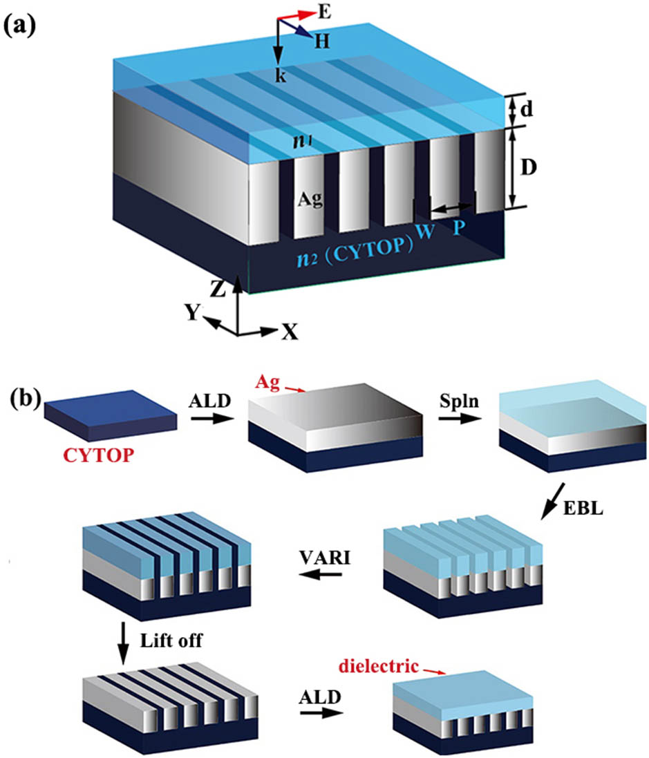
Figure 1(a) illustrates the schematic nanostructure with silver nanoslits implanted in the variable RI substrate called CYTOP. A cover layer of thickness for three variable dielectrics, namely, air, water, and silicon dioxide, is considered to excite the SPR and increase the EOT efficiency. In this work, the dimensional parameters of the nanoslits are as follows: periodic length , width , and depth . Under visible and near-infrared light, the relative permittivity of silver is described by the Drude model as follows[6]: where is the high-frequency bulk permittivity, is the plasma frequency, is the electron damping constant, and is the angular frequency of the incident radiation. The and directions can be considered for the periodic boundary conditions. The light of transverse magnetic (TM) polarization is incident from the top variable dielectric. The numerical simulation has been executed using the finite element method (FEM). To fabricate this metallic grating structure, the methods of physical sputter deposition, reactive-ion etching, and electron-beam lithography (EBL) can be used. Primarily, silver is etched into substrate with EBL. The top variable dielectric is deposited onto the substrate grating easily, or the substrate grating can be placed in the desired environment, as shown in Fig. 1(b).
Figure 1.(a) Schematic of the proposed metallic nanoslit arrays with a top variable dielectric and a CYTOP substrate. (b) Schematic of the fabrication process for the proposed structure.
The periodic metal–dielectric nano-array is investigated in free space with TM waves by using the outlined SPR-based FEM. The top dielectric layer of the structure is silica with the RI of . In Fig. 2(a), the three resonant peaks (, , and ) of the transmission spectrum can be observed because the incident light penetrated the resonant cavity. These resonant peaks correspond to the second-order cavity mode (), SPP-CM mode, and first-order CM (), as illustrated in the magnetic fields of Figs. 2(b), 2(c), and 2(d). The orders of the CM, which are related to the setting of the geometric parameters, denote the values of the nodes in the light field distributions. Figures 2(b) and 2(d) show the magnetic field intensities of and , which focus on the slit walls at the normal incidence wavelength of 1000 nm. Differently, owing to the excitation of SPP on the metal–dielectric and coupling of two modes, the intensities of the magnetic fields are concentrated in the interface between the slits and the different dielectric layers at the second narrow resonant peak (), which is in agreement with Fig. 2(c). The CM and the SPP-CM of the transmission spectrum can be observed by appropriately regulating the relevant parameters.
Figure 2.(a) Transmission spectrum of the top-layer silica with normal incidence. Magnetic field distributions of the device region at (b) , (c) SPP-CM, and (d) .
Furthermore, we design a series of sensors with different geometric parameters to show the transmission properties and the promotion of wavelength sensitivity[23]. The following equation describes SPP characteristics near the dielectric–metal interface[29]: where denotes the dielectric constant of the metal, denotes the RI of the environmental materials, is the mode resonant order, and is the period of the nanostructure. It can be seen from Eq. (2) that the SPP’s resonant wavelength is more sensitive to the period and the duty cycle ()[21]. As a consequence, Eq. (2) mainly governs the excitation and resonance properties of the metallic gratings with stacked multilayers. So, the SPP-CM resonant spectrum shows a phenomenon different from the CM.
The effects of the RIs of the upper and lower media on the optimal transmission enhancement and emission line width are discussed theoretically to explore the performance of the SPP sensors. For this, the RIs of the top layers of the variable dielectrics are assumed to be (air), 1.33 (water), and 1.45 (silica). The first-order transmission spectrum predicted by the model is shown in Fig. 3(a). With an increase in RI, the FWHM and transmission intensities of the variable dielectrics increase simultaneously, and the resonant peak exhibits a certain red-shift. The sensing characteristic can be exploited by selecting the top of the different materials. Moreover, the large ohmic loss hinders the improvement of the EOT in the plasmonic structures, but this loss can be compensated for with nonlinear active media. The optical gain material CYTOP is selected as the compensating medium. The transmission spectra with CYTOP are recorded and analyzed, as depicted in Fig. 3(b). The following equation is used to describe the complex RI: , in which the amount of optical gain can be adjusted by the gain efficiency of constant . Through the interaction of the electromagnetic fields and the optical gain medium, energies can be transferred from the optical gain medium to the EOT resonance of the micro and nano grating structures. In the inset in Fig. 3(b), the RI of CYTOP decreases with an increase in , such that the transmission intensity increases to approximately 0.8 when RI (). The compensation effect of CYTOP on the electromagnetic field loss is remarkable. The gain and EOT resonance of the periodic array system are enhanced, and the effects of energy compensation can improve the performance of the sensor.
Figure 3.Comparison of the transmission spectra of (a) different top materials and (b) gain-assisted materials (the inset provides a clear picture of the peak position).
Figure 4 shows the transmission spectra with oblique incidence angles varying from 0° to 30°. As the angle of inclination of the incident light increases, the transmission intensity decreases gradually. However, the bandwidth also decreases, making wavelength detection more specific. In the near-infrared spectrum, the results indicate that a relatively high transmission and a narrow FWHM can be achieved by changing the incident angles. This step ensures that a better-performing sensor of metal–dielectric periodic array structures can be designed. For instance, the transmittance can reach approximately 0.75 at the maximum angle of incidence of with the other geometric parameters fixed. Meanwhile, the bandwidth of this case is approximately 25 nm.
Figure 4.Transmission spectra for incident angles from 5° to 30°. Different color lines denote distinct incident angles. The inset figure shows the schematic structure of the oblique incidence with variable incident angle . The wavelength of incident light is 1 μm, and the other parameters remain constant.
Under normal excitation, Fig. 5(a) presents the transmission spectra of with varying periods when other parameters remain unchanged. Figure 5(b) shows that with an equidistant increase in the period the transmission spectra exhibit a slight red-shift about periodic values from 400 to 800 nm. In particular, a decreased and narrowed transmission of CM is observed as the period increases with the same geometrical parameters. However, the SPP-CM resonant peak acts exactly opposite, and the trend of the red-shift is more obvious, so different sensing characteristics can be achieved. Furthermore, previous work discusses the resonance modes based the approach of regulating the duty cycle. Thus, the distribution patterns of the transmission spectrum shown in Fig. 6 are examined. The transmittance increases and reaches approximately 0.9 with , and the spectral line becomes sharper. This phenomenon produces a significant modulation effect because the plasmonic resonances between the metal and dielectric interfaces are improved. With an increase in , the transmission spectrum in the near-infrared region exhibits a slight blue-shift. On this basis, a large duty cycle should be selected appropriately to enhance the performances of sensors.
Figure 5.(a) Transmission spectra of the first-order CM of the periodic metal structure with different values of period. (b) Transmission intensities as a function of the corresponding wavelength () and period.
Figure 7(a) shows the transmission spectra of the with an increasing nanoslit depth from 360 to 560 nm. The figure substantiates the influence of the nanoslit depth on the transmission intensity and clearly presents the relationship between depth and wavelength. The resonant CM of shifts to longer wavelengths gradually, and the transmission intensity is doubled. An apparent red-shift occurs in the transmission spectra, and its effect becomes obvious near the long wavelength because of the stability of the atomic groups considered in the calculations. Generally speaking, nanoslit depth can be varied to determine the performance of a variable dielectric–metal–variable substrate sensor in terms of wavelength sensitivity and FOM. This section assumes that all variables, except for nanoslit depth, should be kept unchanged, which is the principal influencing factor used to detect the change in sensitivity () at different peak wavelengths and adjustable RIs of the substrate. Figure 7(a) shows that the FWHM will increase nonlinearly with an increase of depth, owing to the transmission of light at the metal array, which will cause the improvement of the gain effect gradually. As shown in Fig. 7(b), the wavelength sensitivity profile is drawn by the blue curve. With the slight increase of RI, the sensitivity will be enhanced, which will exceed 800 nm/RIU at . However, the FOM (S/FWHM) decreases gradually, as indicated by the red polyline shown in Fig. 7(b). The increase in FWHM is faster than the increase in sensitivity. This minimal change does not affect the performance of the SPP sensors, and it can be easily detected. Therefore, the appropriate parameters can be selected to obtain the desired effect. This work provides the basis for designing high-sensitivity plasmonic metal–dielectric sensors. The EOT and high sensitivity are achieved and strengthened by optimizing the parameters, particularly the nanoslit depth based on the variable dielectric–metal–variable substrate design of the periodic metallic slits.
Figure 7.(a) Transmission intensity as a function of wavelength () and slit depth. (b) Wavelength sensitivity of the resonance peak of and its FOM as functions of depth. Other parameters: normal incidence, , , and .
In this Letter, a variable dielectric–metal–variable substrate sensor is proposed and demonstrated. Subtle changes in RIs of the upper and lower dielectrics can affect the transmission intensity significantly and reduce inherent loss of the sensor. Furthermore, as a plasmonic periodic grating sensor, the structure achieves the wavelength sensitivity higher than 800 nm/RIU or FOM of more than 45 over a wide spectral range. This proposed sensor shows considerable potential for extensive applications.