Abstract
Advanced electronic materials are the fundamental building blocks of integrated circuits (ICs). The microscale properties of electronic materials (e.g., crystal structures, defects, and chemical properties) can have a considerable impact on the performance of ICs. Comprehensive characterization and analysis of the material in real time with high-spatial resolution are indispensable. In situ transmission electron microscope (TEM) with atomic resolution and external field can be applied as a physical simulation platform to study the evolution of electronic material in working conditions. The high-speed camera of the in situ TEM generates a high frame rate video, resulting in a large dataset that is beyond the data processing ability of researchers using the traditional method. To overcome this challenge, many works on automated TEM analysis by using machine-learning algorithm have been proposed. In this review, we introduce the technical evolution of TEM data acquisition, including analysis, and we summarize the application of machine learning to TEM data analysis in the aspects of morphology, defect, structure, and spectra. Some of the challenges of automated TEM analysis are given in the conclusion.Advanced electronic materials are the fundamental building blocks of integrated circuits (ICs). The microscale properties of electronic materials (e.g., crystal structures, defects, and chemical properties) can have a considerable impact on the performance of ICs. Comprehensive characterization and analysis of the material in real time with high-spatial resolution are indispensable. In situ transmission electron microscope (TEM) with atomic resolution and external field can be applied as a physical simulation platform to study the evolution of electronic material in working conditions. The high-speed camera of the in situ TEM generates a high frame rate video, resulting in a large dataset that is beyond the data processing ability of researchers using the traditional method. To overcome this challenge, many works on automated TEM analysis by using machine-learning algorithm have been proposed. In this review, we introduce the technical evolution of TEM data acquisition, including analysis, and we summarize the application of machine learning to TEM data analysis in the aspects of morphology, defect, structure, and spectra. Some of the challenges of automated TEM analysis are given in the conclusion.1. Introduction
Table Infomation Is Not Enable
The qualities of electronic materials can have a considerable impact on the performance of electronic devices[1-3]. Even a nanoscale defect could result in the failure of a device[4, 5]. Therefore, comprehensive analysis of the electric material is indispensable. The transmission electron microscope (TEM) has been widely applied for the structure-property study of materials and devices due to its high-spatial resolution and versatile characterization abilities[6, 7]. With the developed aberration correction technology, the spatial resolution of the TEM has been improved to 0.5 Å. This allows scientists to directly observe the atomic configuration of materials[8, 9]. In addition to morphology, TEM can also provide structure, composition, and even valence state[10-13]. The recently developed in situ TEM technology also provides a real-time method to characterize and manipulate materials with external stimuli, such as electrical, mechanical, thermal, optical fields, and liquid/gas environments[6, 14-17].
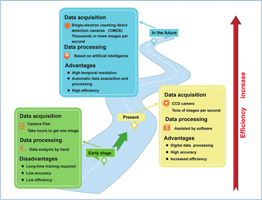
The sample information obtained by TEM characterization is presented in the form of images[18-22]. Great progress has been made in the acquisition and processing of TEM images, as shown in Fig. 1. In the early stage, the TEM images were captured by camera films that have to be developed to get the sample information. However, this process is complicated, time-consuming, and requires training to obtain a qualified image[23-27]. The data is not digitalized and the image analysis has to be calculated by hand, which results in low accuracy and efficiency. With the improved performance of photosensitive devices and the increased pixel density, CCD (charge-coupled device) cameras replaced film cameras for TEM image recording. The CCD camera converts electronic signals into photon signals through scintillators. Then, the photon signals activate the silicon epitaxial layer and generate charges. The accumulated charges are converted into voltage and stored in memory, forming digital images. The digitalized TEM image can easily be processed by professional software, such as digital micrograph and so on, which greatly improves the accuracy and efficiency of TEM data analysis[28]. The forthcoming TEM camera based on complementary metal oxide semiconductor (CMOS) could directly detect electron signals without a scintillator[29-32]. This dramatically improves the efficiency and avoids the loss of signals from scintillators, which promotes the quality of imaging, especially in the aspects of signal-to-noise ratio and low dose imaging[33, 34]. TEM methods have also been adopted to study low dimensional materials[35-39]. In addition, artificial intelligence (e.g., machine learning) will be widely applied to automatically process a large quantity of in situ TEM images with high temporal resolution.

Figure 1.(Color online) The evolution of TEM data acquisition and processing.
Unlike the color-scaled images in a natural scene, TEM images that are formed by an electron signal are grayscaled maps. In addition, the TEM image has high statistical noise, low contrast, and blurred boundaries, resulting from conditions such as the thickness of the sample, the sensibility of the materials to electron beam, and so on. To mitigate the damage of the sample induced from the electron beam irradiation, a common solution is to reduce the shooting time at the sacrifice of resolution[40].
Analysis of TEM data is time-consuming and requires specialized knowledge, which mainly results from two aspects. First, the features in TEM images are usually complex and vague, which increases the difficulties for fast and accurate information extraction. Second, a large number of TEM images can easily be obtained for each TEM experiment, especially for video streams that are recorded during in situ TEM experiments. Even at the present stage, more than a thousand images can be acquired within several minutes. These issues have led to the demand for a way to efficiently analyze large and complicated TEM datasets[41-43].
The resurgence of machine learning has greatly impacted image recognition and offers an excellent opportunity for automated TEM data analysis[44-49]. Machine-learning methods are mathematical models that are used to help a computer learn to automatically process data, imitating the methods that humans use. Machine learning is generally divided into three subcategories: supervised, unsupervised and reinforcement machine learning. The difference between supervised and unsupervised methods lies in whether or not the dataset is labeled. The reinforcement method learns from trial and error through a feedback loop. Neural networks are a fast-developing machine-learning method that provide high accuracy in image recognition and require less human intervention. The first convolution neural network (CNN) model, LeNet, was reported by LeCun et al. in 1989, and adopted local response and pooling to enhance performance of the network[50]. Subject to the computer power at that time, machine learning did not become popular until the AlexNet came out in 2012. The network imported dropout and data augmentation to avoid overfitting, and rectified linear units (ReLUs) were used as a new activation function, which was a big step forward in computer vision[51]. Recently, machine learning based methods have been successfully used in medical and natural image recognition[52-54].
In the field of TEM high-throughput images analysis, tasks concern segmentation or classification of specific characteristics of interest from material images. Neural networks for automated analysis of TEM images mainly include a CNN algorithm, a fully convolution network (FCN) algorithm and a U-Net algorithm. The CNN is determined by three components, the convolutional layer, pooling layer and a fully-connected (FC) layer. The first two layers produce feature maps and reduce dimensionalities. The last, FC, layer produces a one-dimensional vector for classification tasks. Unlike CNN scarifying of the spatial information of input images, the FCN performs classification for each pixel of the image by replacing the FC layer with the convolutional layer. The U-Net is an improved FCN structure with encoder and decoder networks, which has symmetric skip-connected contracting and expansive paths to capture features and for accurate localization. The U-Net can be trained by the available labeled samples with higher efficiency. U-net has been widely adapted in medical image identification, due to its efficiency and precision. U-net is comparatively more adaptable for TEM image segmentation tasks, which is similar to that of medical images tasks.
Efforts have been made to integrate automatic approaches with imaging processing to cope with the obstacles existing in TEM image analysis[55-61]. As shown in Fig. 2, the publication trend suggests a sharp increase number of studies using the machine-learning method for TEM image analysis. Along with the development of computing power, the automatic analysis of TEM imaging by machine learning is very promising and still in its initial stages, and deserves more effort. Machine learning has contributed to the analysis of the nanomaterial images by TEM characterization in the aspects of defect, morphology, structure, and spectra, as shown in Fig. 3[62-67]. The main information of the typical works that have been published recently is summarized in Table 1.
Figure 2.(Color online) Publications from the Web of Science with the keywords of TEM and machine learning.
Figure 3.(Color online) Application of artificial intelligence for high-efficient processing of various TEM datasets. FCN, CNN, and UDN are short for fully convolution network, convolutional neural network, and unsupervised deep network, respectively.
In this review, the recent developments of the TEM data analysis based on machine learning are summarized. We first present the background and technique evolution of the TEM data acquisition and analysis. Then, TEM data analysis is discussed in detail from four aspects: morphology, defect, structure, and spectra by the application of various neural networks. Finally, in the conclusion we state the challenges of artificial intelligence assisted TEM data analysis.
2. Machine learning based analysis of TEM
2.1. Analysis of defects
Meanwhile, 2D materials with ultrathin geometry, large specific area, and rich physical properties are widely applied in the fields of electronics, sensors, energy storage and conversion[73-79]. The study of local defects has for a long time been an important research field in material science because it can greatly affect the physical and chemical behaviors of 2D materials, even with a limited number of dopants or vacancies[80]. The defects of a 2D material could influence the semiconductor carrier type, the catalytic, and optical properties[81-85]. In terms of defect analysis, determining atom position is indispensable[86]. Scanning transmission electron microscopy (STEM) is an appropriate characterization method for atomic-defect investigation due to two aspects: the sub-angstrom spatial resolution and the contrast sensitivity to the square of the atomic number[87, 88]. STEM characterization uses a focused electron beam to probe each atom of the TEM sample and then collect the scattered electron signals to form the image contrast. An element with a higher atomic number can diffract the incident electron beam more effectively, which results in higher contrast. For the traditional manual processing method, processing a large number of in situ STEM images is nearly impossible. Machine learning based approaches are highly effective and are increasingly applied in the tasks of atomic defects localization, identification, and classification.
Ziatdinov et al., for instance, take advantage of a weakly-supervised FCN to identify defects, including vacancies and doping atoms in STEM images. The FCN model contains an encoder-decoder structure, which turns the last fully-connected layer of the conventional CNN into a convolution layer, and outputs the probability mapping of each pixel corresponding to various atoms or defects; as shown in Fig. 4(a). This approach could start with a few labeled general defects and can identify complex defects, even those not in the training set, requiring less human intervention[72].
Figure 4.(Color online) The introduction of a neural network in the analysis of atomic defects[72]. (a) Schematic architecture of a CNN with an encoder-decoder structure. (b) Location of carbon atoms of graphene. (c) The extracted dopant Si atoms and, in this way, the classification between 3-fold and 4-fold Si defects is conducted. (d) The evolution of the same Si dopant on the time scale. (e) Classification of defect types. (f) Extraction of the defect from STEM images.
The quantity and quality of the labeled TEM dataset are critical for training a network with high accuracy. However, there is still lack of high-quality labeled TEM datasets. As an alternative to labeled experimental data, the simulated TEM data with accurate ground truth is easier to obtain. The multislice calculation-based algorithm is usually applied for TEM data simulation, including STEM images[60, 64]. The simulated STEM images are generated to train the model, and experimental images are used as the test dataset. After the center and contour of individual atoms, the atom positions and the chemical bond configurations can be explored; as presented in Figs. 4(b) and 4(c). By analyzing each frame of the in situ STEM images, the defect evolution with the variation of time is quantitively studied Figs. 4(d)−4(f).
Using the FCN algorithm, the atom positions and types in a lattice are recognized with high accuracy, enabling effective defect determination. The presented algorithm can be extended to other automatic TEM image analysis that relates to the atomic position.
Similar to medical images, TEM images usually suffer from background noise and vague boundaries. According to the advanced algorithm for medical image recognition, reducing background noise during the image analysis is required.
To reduce the raster distortion during STEM image acquisition, fast imaging speed is required. This results in a low signal-to-noise ratio (SNR)[64]. Improving the SNR before applying the CNN-based algorithm for STEM image processing could increase the accuracy of the results. Yang et al. innovatively adopt an automated method based on two neural networks to improve the image SNR and complete the image segmentation of atomic defects and dopants in 2D transition metal dichalcogenides (TMDs)[64]. A CNN-based algorithm (supervised learning) with a dilated convolutional kernel is first applied as a denoiser to the raw experimental images. Simulated ADF STEM images obtained by multislice calculations are used to get a high-quality training dataset, and the noise signal is simulated by the Poisson distribution. Using this method, the SNR and the atomic contrast of the experimental STEM image are enhanced, as shown in Figs. 5(a)–5(c). From high-contrast input images, various defects (including atom doping and atomic vacancies) are clearly identified in the V-WSe2 by a U-Net algorithm with an accuracy of up to 98%. In addition, the dynamic behaviors of different defects under e-beam stimulus can also be unveiled, as shown in Figs. 5(d) and 5(e).
Figure 5.(Color online) Introduction of CNN-based algorithm for atomic-scale identification of point and line defects[61, 64]. (a) A CNN as a denoiser process. (b, c) Comparison of the signal-to-noise between the unprocessed and processed images. (d) Defect mapping of STEM image. (e) The statistics of Se vacancies and V dopants change according to the electron beam irradiation time. The scale bar is 5 nm. (f) The architecture of U-Net. (g, h) The border recognition of a nanopore.
The U-Net model has been widely used in processing medical images and it shows excellent performance in defect classification. The U-Net algorithm has skip connections and concatenation operation that could identify features of different scales and achieve good accuracy with a small dataset; as shown in Fig. 5(f)[52]. In addition, U-Net adopts an overlap-tile strategy, which generates no overlapping range and conducts a seamless segmentation to input of any size. This strategy benefits the learning efficiency, especially in scenarios with limited annotated training datasets or unscalable raw images. Except for the point defect recognition, a line defect (e.g., a nanopore border) can also be identified and analyzed by the U-Net algorithm; as shown in Figs. 5(g) and 5(h)[61]. The CrTe2 nanopore healing process induced by the synergistic effect of electron beam irradiation and heating field is captured by in situTEM. Over 1300 TEM images that were labeled by hand are used for U-Net training. After 100 epochs training, the DICE metric reaches 93.17%, showing an effective line defect recognition by the U-Net algorithm.
The rapid development of machine learning aided TEM data recognition makes the real-time characterization and analysis of defects during the in situ TEM operation possible. The immediate feedback of the defect evolution information could further guide thein situ TEM experiment along a planned road, which accelerates material mechanism discovery with high efficiency.
2.2. Analysis of the morphology
Many efforts have been made to study the morphology of nanoparticles (NPs), which govern the physical and chemical properties of the nanomaterial. The morphology of a sample reflects the types of its exposed surfaces, which has an impact on its catalytic activity[89, 90]. The morphology evolution process also unveils the stability or growth kinetics of the NP[91-97]. TEM can characterize the morphology of nanomaterial with atomic resolution. The 2D projections of 3D particles that are obtained from TEM are usually studied for their morphological features. In general, NP analysis includes three stages: morphology capture, filtering, and shape classification. The foreground and the background need to be separated to locate and isolate the individual particles. Then, in the dataset of detected targets, filtering is required to eliminate the superimposed or abutted particles that may be wrongly recognized and disturb the statistical result. Finally, the particles are put through the classification process and the distribution map is presented. The descriptors, based on which the particles are divided, primarily include solidity, area, convexity, eccentricity, circularity, aspect ratio, and angular distance. Two approaches are introduced as the determined attempts of NPs.
A completely unsupervised method, called AutoDetect-mNP, was introduced by Wanget al. to identify the shape attribution of Au NPs (Fig. 6(a)). To differentiate the individual particles and the background, the algorithm adopts K-means image segmentation. During the TEM imaging process, Au particles (due to their high mass and high lattice packing efficiency) show intense interaction under an e-beam from a TEM, thus generating a strong contrast in the images. Partly because of this high contrast between the foreground and the background, the adopted simple computer vision approach proves sufficient for this stage. The nanorods are classified after going through a filtration for convexity and solidity. For the classifier, this study uses a combination of K-means clustering and naive Bayes classification to serve the purpose of being totally unsupervised; shown in Fig. 6(b). As a result, this approach has a great performance for both efficiency and accuracy when compared to the previous methods for the analysis of Au nanorods. It also reduces the bias by reducing human input. However, when adapted to materials that show lower contrast, such as palladium (Pd) and cadmium selenide (CdSe) particles, the unsupervised K-means image segmentation may not be good enough for identification.
Figure 6.(Color online) Introduction of two machine learning based methods in morphology analysis of gold particles[63, 68, 70]. (a, b) A complete unsupervised clustering algorithm utilized in classification of gold nanorods. (c) A GA containing various image analysis methods as genes to explore the morphological characteristics of NPs. (d) NPs segmented by U-Net with boundaries. (e) The intensity of the four types of NPs and the background in the TEM images explored by U-Net. (f) Boundaries of NPs colored to their local etching rates and the etching time indicate the height. (g) The three etching stages defined by the relationships between the etching rate and curvature.
A supervised method is a promising solution to pursue high precision in machine learning based NP detection. Leeet al. explored an approach based on a genetic algorithm (GA) to analyze the morphological properties of NPs, with a precision as high as 99.75%; as shown in Fig. 6(c)[70]. Using natural selection for reference, the GA filtrates the genes according to a specified standard, and only those with the best performance can be the survivors. The leftover genes go through the same course of evolution, mutation, and filtration. The surviving genes are considered as the optimal result. In this study, locating the NPs is not only the case, but properly separating or deserting the superimposed particles based on the extent to which they are abutted is also needed. Various imaging processing methods (i.e., thresholding and watershed transform) can be used to compose the variables. The aim is to explore the optimal variable-variable combination utilized in the morphology analysis in the NP systems. High-scoring images (genes) of every round are stacked in the algorithm to pile up the detected NPs, and thus augment the statistical significance. After the images are filtered with the GA algorithm and processed with the optimal composition of various imaging analysis techniques, they are clustered and their distribution is analyzed statistically to be ready for further research.
Yao et al. introduced a U-Net model to extract information of physical and chemical properties[63]. Their machine model was fed with the training set constituted by simulated liquid-phase images. Beer’s law, Poisson noise, and Gaussian noise are considered to simulate the liquid-phase imaging under e-beam. First, the boundaries of NPs in each frame in the TEM video are located, based on which the intensity of four categories of gold nanorods and background is calculated; as shown in Figs. 6(d) and 6(e). Second, during etching, the nanorod boundaries are tracked and marked colored to their curvature. The height and etching rate are monitored in real time. Finally, from the statistical analysis of the big dataset, three stages are concluded, showing how the etching rate changes. Its interrelation with curvature is shown in Figs. 6(f) and 6(g).
In the liquid-phase TEM video, the contrast fluctuation appears to be a primary challenge. The different thickness and orientation of each nanorod result in contrast variation, even in the same image. Even for the same particle, the motions at the time scale lead to a shift in the intensity diagram. Such fluctuation cases happen randomly and inevitably, and have been longstanding obstacles in liquid-phase TEM movie processing. Due to the unique skip-connection structure, the U-Net algorithm includes various factors, such as intensity, morphology, and local surroundings in the process of segmentation, while the previous thresholding approaches include only the intensity of the pixels. U-Net structures are suitable in segmentation tasks for liquid-phase TEM images that have contrast fluctuations and low SNR. The advantages of the application of U-Net models are the robust segmentation, high tolerance over low-quality images, intensity fluctuation and many other defects of the sample. The robust segmentation of the U-Net favors the precise and efficient tracking of boundaries and analysis of the particle properties.
For the morphology of materials, the thickness is closely related to the intrinsic properties, such as bandgap and optical properties[98-100]. Both HRTEM and the recently developed 4D-STEM images contain the thickness information of the TEM sample. The HRTEM and 4D-STEM are TEM imaging modes with atomic spatial resolution. The HRTEM uses a parallel electron beam to form images, and the phase contrast is generated from the interference of electrons that interacted with and without the sample atoms. The 4D STEM image uses a pixelated signal detector to get the conventional 2D STEM image and 2D diffraction pattern at the same time to form the 4D-STEM data. Compared with the traditional STEM, 4D-STEM provides more information for sample property extraction[101-103].
Since the sample is projected as 2D in TEM images, the recognition of column heights out of 2D images has been a popular topic. Here, two works are introduced to evaluate the atom numbers in the atom columns that present the thickness of the sample. Two different convolutional networks, a regression CNN (r-CNN) and a classification CNN (c-CNN), are used in these two works for the recognition of HRTEM and STEM images, respectively. The two models are trained and applied to estimate the column heights of metallic NPs. The results of the two methods are compared to clarify their suitability.
First, Ragone et al. detect the atomic column heights of metal particles with two automated methods based on CNN[69]. Simulated TEM images with the labeled ground truth are calculated by QSTEM[104]. The brief architecture and the result example of the column height prediction of the model are shown in Figs. 7(a) and 7(b). Based on HRTEM images, both the networks determine the heights based on the values of pixels. In the classification CNN model, the output of the network is a probability map of the thickness of NPs, indicating the discrete classes of the values of their heights. In this study, a maximum height of 15 atoms is considered to be sufficient, and the output classes of thickness are from 1 to 16. The so-called regression-based model is not usually attributed to a standard segmentation task. Unlike the discrete classes in the classification output, the pixel values of TEM images are deemed to have a continuous decrease from the column’s center to background. After being trained with simulated TEM images, the model correlates each pixel to a value of the predicted height. From the comparison of the two methods, the regression-based model is reported to be approximately 10% more accurate than the classification model. The contrast of HRTEM is sensitive to the degree of defocus. The influence of defocus to image recognition accuracy is evaluated as shown in Fig. 7(c). The low defocus and low dose images have relatively low accuracy.
Figure 7.(Color online) Application of machine learning based methods in the analysis of atomic column heights. (a) A CNN illustration as an example of the supervised network utilized in the analysis. (b) Comparison between ground truth and prediction after regression and classification on STEM images. (c) Results of the network with various defocus values and electron dose. (d) The sub-unit cell calculated and mapped from a 4D-STEM dataset. (e) Comparison between c-CNN and r-CNN measurement and HAADF estimation.
Second, in Zhang et al. the convergent beam electron diffraction (CBED), namely 4D STEM, is adopted to assist the CNN-based thickness detection[60]. As is shown in Fig. 7(d), the positive-averaged CBED (PACBED) pattern of Sr particles is obtained and used to generate a thickness prediction map through a CNN. Both the c-CNN and the r-CNN determine the number of unit cells overlapping on one column. In Fig. 7(e), the result of c-CNN is listed in the red frame and the r-CNN is in the blue frame. A comparison of the two models shows that both models are sufficient on sample thicknesses within 40 nm, and have varying degrees of falling in accuracy as the thickness increases. The r-CNN performs better in fine estimation of thickness but requires more effort to be trained. However, the c-CNN has lower precision, especially for thick samples.
2.3. Structural analysis
Crystal structure governs material properties, and the carbon allotropes are typical examples. Even for carbon nanotubes (CNTs), the different structures that are determined by chiral indices show distinct electric properties. Furthermore, 2D materials with the same composition could have different electrical properties[105, 106]. For example, the 2H phase MoS2 is semiconductive and the 1T phase MoS2 is metallic[107, 108]. The diffraction mode of TEM is widely used to determine crystal structures, from the microscale to the nanoscale. The diffraction pattern that conforms to Bragg's law has a bright contrast. The positions of the diffraction spots with respect to the center transmission spot determine the crystal structure. HRTEM unveils atomic configuration and can also be used for structure studies, such as chiral indices.
The classification of crystal structures can benefit from the use of neural networks. Ziletti et al. adopted an automated method to classify the structure of a dataset of 3D materials based on their crystal symmetry[62]. To skirt the much prior expertise that was traditionally required in classification algorithms, this research uses the ConvNet and the architecture that is shown in Fig. 8(a). ConvNet performs well in image recognition and can learn features in classification. The first step to analyze 3D structures in 2D images is to find a proper descriptor to represent the material. Diffraction patterns in x-axis, y-axis and z-axis overlapped in one image delegated by red, green and blue are introduced to represent the crystal structures[62]. Note that the quadrature axis is arbitrary, and little is required to be known about the sample’s crystal symmetry. It is the crystal structure rather than the atomic composition that matters in the representation patterns, which makes this approach suitable for a good classifier because it differs the representations of diverse classes while reducing the difference between structures of the same class due to its robustness to defects. Given that the crystal structures have been transformed into more understandable diffraction fingerprints, 90% and 10% data are used for training and testing, respectively. Simulated crystal structures coupled with random displacements, substituting atoms and vacancies are combined to create an ideal dataset containing defective systems. Although the neural network itself in general figures out the features to be used in the task, it can be inferred that the classification is conducted based on the diffraction peak and their positions. As is shown in Figs. 8(c) and 8(d), the network shows robustness in tasks to categorize crystal structures, even in the case of structural transitions.
Figure 8.(Color online) Application of CNN in structure analysis. (a) The workflow of deploying a neural network model to automatically classify structure. (b–d) Two-dimensional diffraction patterns of different crystal structures are divided into eight classes in SAED. (e) An illustration of a CNN(LeNet-5) with a computer-simulated training dataset. (f) Comparison between manual and automatic classification. (g) Correlation matrix of the results of the two methods.
The properties of CNT are primarily determined by chiral indices[109, 110]. In the analysis of chiral indices, the diameter and the chiral angle are the focus of research, which can be assisted by machine learning-based methods. Georg Daniel Forster et al. conducted the analysis task for chiral indices with the help of a neural network based on the classical LeNet-5, which proves to be effective on the HRTEM image of CNTs shown in Fig. 8(e)[71]. Trained by simulated images with consideration of defects, this method was able to identify and classify the diameter of the nanotube by extracting of a contrast intensity profile (i.e., the distance between the dark and bright fringes). The chiral angle is measured through a Fourier Transform (FT). From the correlation matrix of the manual and automated results, especially in low diameter nanotubes, the machine learning-based method shows high accuracy in chiral structure determination of CNTs; as shown in Figs. 8(f) and 8(g).
Diffraction pattern identification is one of the most widely used operations during TEM characterization. The crystal structure determination algorithm can be extended for automatic diffraction pattern identification, which is of great significance when building an intelligent TEM operation system.
2.4. Spectra analysis
The local composition and the atom valence state are important information that influence the properties of a material. There are two methods for chemical analysis in TEM: energy-dispersive X-ray spectroscopy (EDX) and electron energy-loss spectroscopy (EELS). Both of them can be obtained in the STEM mode. The EDX is the characteristic X-ray signal that is emitted from the ionized atoms that are stimulated by the incident electron beam. EDX is collected in the STEM mode and has a nanoscale even atomic-scale resolution. The EELS signal results from the inelastic scattering interaction between the incident electron and atoms in the TEM sample.
EELS is a powerful tool to probe local chemical information with atomic resolution[111-115]. The spatial environment of an electron in the TEM sample can be obtained by analyzing the energy loss of the diffracted electron beam[116-118]. The analysis of massive generated EELS data is still challenging. To tackle this challenge, Roccapriore et al. presents two convolutional neural networks to establish a relationship between the NP geometries and the plasmon responses[65]. In this way, spectral response can be determined by analyzing the structural imaging, which takes much less time to generate when compared to the spectral spectrum from the spectroscopy. In the Im2spec network, when the local subimages around specific locations (special descriptor) are input, the EEL spectra associated with the local configuration are presented; as shown in Fig. 9(a); and vice versa, in the spec2im network in Fig. 9(b), the spectra descriptors are considered as features, and the images of local configuration as targets are predicted by the network. In general, the mutual relationship between local configurations of NPs and the corresponding plasmon spectra diagram is established in the study. In many common cases, the result can be considered to be a basis in theoretical models. While for models that are not suitable to directly adopt this result, the establishment procedure is of referential significance. Although the obtained model is not suitable for the direct analysis of other TEM datasets with similar features, the network trained with this methodology could be applied as a pre-trained model for transfer learning in new TEM data analysis. Moreover, the pretreatment of training dataset and optimization of the network structure can improve the generalization ability of the model[119, 120].
Figure 9.(Color online) Introduction of the use of a neural network to explore the correlative laws between local geometries and plasmon responses[65]. (a) The im2spec network, in which subimages are taken as features and spectra are taken as targets. (b) The spec2im network, which is trained with HAADF spatial descriptors and corresponding spectral descriptors, similar to the im2spec network. However, the spectra are used as features and subimages are used as targets.
EDX spectra can be obtained during STEM imaging with a high-spatial resolution for composition-related studies of nanomaterials. Due to the sensitivity of nanomaterials to the STEM electron beam, the acquired EDX spectra have to be limited and the scan speed has to be fast to reduce the electron-beam-induced defects. These experimental conditions result in a small number of obtained EDX spectra with high background noise, which is a considerable challenge for EDX spectra analysis. Han et al. offers two unsupervised deep networks to tackle these problems, a denoising network and a two-step neural network, which generate high-resolution 3D EDX spectra; as shown in Figs. 10(a)–10(c)[67]. The two-step neural network first produces an intermediate noisy 3D reconstruction using the raw EDX projection data and then the projection data obtained from the noisy 3D reconstruction is enhanced using CNN. The consistency restriction is applied to guarantee that the calculated EDX spectra conform to the experimental data at the same angle. The two-step neural network can be applied to generate a large quantity of EDX spectra, even at the unmeasured angles. Because only the experimental data are used as the restrict condition, the neural network does not need a large number of labeled spectra for supervised training. Automatic EDX spectra processing and 3D reconstruction can be used in the chemical-property analysis of nanomaterials
Figure 10.(Color online) The work flow of the 3D construction of STEM energy-dispersive X-ray spectroscopy (STEM-EDX) by deep learning[67]. (a) Collection of raw EDX experimental maps. (b) A denoising network to improve the noisy EDX maps. (c) Unsupervised deep network to generate high-quality 3D reconstruction.
3. Conclusion
In this paper, machine learning for in situ TEM is reviewed. Automated TEM data analysis has been summarized from the aspects of morphology, defect, structure, and spectra by machine learning. The merits of machine-learning methods for the corresponding data analysis tasks are discussed. Although the application of machine learning for TEM data analysis is a vibrant field and it is developing quickly, there are still several challenges, as follows:
(1) Natural and medical images have many datasets for network training and testing. However, there are few TEM datasets. Because of the data-driven feature, high quality and large quantities of TEM datasets are critical to achieve a trained network that has good performance. Image data augmentation of a manually annotated database could be a solution to this problem. Some studies have created simulated TEM images to meet the requirement of a much larger database with less labor. In addition, optimizing a network structure so that it requires less training data and still maintains performance could be an alternative solution to this problem.
(2) Machine-learning algorithms for TEM data analysis are usually optimized for a specific scenario. Models and network structure for TEM usually have so far been tailored for certain types of microscope images and materials. However, methods restricted in these conditions could lose robustness when adapted to new cases. Therefore, algorithms suitable for more general TEM data analysis need to be developed. At the present stage, the automation TEM data analysis is mainly focused on material. Electronic device characterization data obtained by in situ TEM and corresponding machine learning based data analysis (especially for the interfaces) are required.
(3) With the increased time and spatial resolution of in situ TEM characterization, the large amount of data that are generated in a short time create a challenge of data transfer and storage. Recently, compressing large amounts of data for electron microscopy by deep compressive sensing learning has been reported[121].
(4) Most of the machine-learning methods adopted in analysis of TEM images are supervised. The unavoidable human bias of this method generates deviations in results, even from experts. Therefore, approaches that have fewer human interactions or unsupervised-algorithm aided methods should be developed for use in TEM.
Acknowledgements
This work is supported by NSFC under Grant Nos. 62074057, 62174056, Projects of Science and Technology Commission of Shanghai Municipality Grant Nos. (19ZR1473800, 18DZ2270800). ‘Shuguang Program’ supported by Shanghai Education Development Foundation and Shanghai Municipal Education Commission, and the Fundamental Research Funds for the Central Universities.
References
[1] A Avsar, A Ciarrocchi, M Pizzochero et al. Defect induced, layer-modulated magnetism in ultrathin metallic PtSe2. Nat Nanotechnol, 14, 674(2019).
[2] M Zhou, W Wang, J Lu et al. How defects influence the photoluminescence of TMDCs. Nano Res, 14, 29(2021).
[3] J Jiang, Z Ni. Defect engineering in two-dimensional materials. J Semicond, 40, 070403(2019).
[4] X Chen, F Du, C Wang et al. Direct visualization of breakdown-induced metal migration in enhanced modified lateral silicon-controlled rectifiers. IEEE Trans Electron Devices, 68, 1378(2021).
[5] X Wu, C Luo, P Hao et al. Probing and manipulating the interfacial defects of InGaAs dual-layer metal oxides at the atomic scale. Adv Mater, 30, 1703025(2018).
[6] C Luo, C Wang, X Wu et al. In situ transmission electron microscopy characterization and manipulation of two-dimensional layered materials beyond graphene. Small, 13, 1604259(2017).
[7] R G Mendes, J Pang, A Bachmatiuk et al. Electron-driven in situ transmission electron microscopy of 2D transition metal dichalcogenides and their 2D heterostructures. ACS Nano, 13, 978(2019).
[8] Z Dong, Y Ma. Atomic-level handedness determination of chiral crystals using aberration-corrected scanning transmission electron microscopy. Nat Commun, 11, 1588(2020).
[9] N J Zaluzec. The influence of Cs/Cc correction in analytical imaging and spectroscopy in scanning and transmission electron microscopy. Ultramicroscopy, 151, 240(2015).
[10] Y Lin, M Zhou, X Tai et al. Analytical transmission electron microscopy for emerging advanced materials. Matter, 4, 2309(2021).
[11] J Zhang, Y Yu, P Wang et al. Characterization of atomic defects on the photoluminescence in two-dimensional materials using transmission electron microscope. InfoMat, 1, 85(2019).
[12] B H Kim, J Yang, D Lee et al. Liquid-phase transmission electron microscopy for studying colloidal inorganic nanoparticles. Adv Mater, 30, 1703316(2018).
[13] Z Fan, L Zhang, D Baumann et al. In situ transmission electron microscopy for energy materials and devices. Adv Mater, 31, 1900608(2019).
[14] X Yang, C Luo, X Y Tian et al. A review of in situ transmission electron microscopy study on the switching mechanism and packaging reliability in non-volatile memory. J Semicond, 42, 013102(2021).
[15] C Zhang, K V Larionov, K L Firestein et al. Optomechanical properties of MoSe2 nanosheets as revealed by in situ transmission electron microscopy. Nano Lett, 22, 673(2022).
[16] N de Jonge, L Houben, R E Dunin-Borkowski et al. Resolution and aberration correction in liquid cell transmission electron microscopy. Nat Rev Mater, 4, 61(2019).
[17] H Xu, X Wu, X Tian et al. Dynamic structure-properties characterization and manipulation in advanced nanodevices. Mater Today Nano, 7, 100042(2019).
[18] J S Cai, R Cai, Z T Sun et al. Confining TiO2 nanotubes in PECVD-enabled graphene capsules toward ultrafast K-ion storage: in situ TEM/XRD study and DFT analysis. Nano-Micro Lett, 12, 123(2020).
[19] R B Wang, Z T Song, W X Song et al. Phase-change memory based on matched Ge-Te, Sb-Te, and In-Te octahedrons: Improved electrical performances and robust thermal stability. Infomat, 3, 1008(2021).
[20] Y H Wang, J B Pang, Q L Cheng et al. Applications of 2D-layered palladium diselenide and its van der Waals heterostructures in electronics and optoelectronics. Nano-Micro Lett, 13, 143(2021).
[21] Y L Wu, R R Gaddam, C Zhang et al. Stabilising cobalt sulphide nanocapsules with nitrogen-doped carbon for high-performance sodium-ion storage. Nano-Micro Lett, 12, 48(2020).
[22] H Zhang, Y Yang, H Xu et al. Li4Ti5O12 spinel anode: Fundamentals and advances in rechargeable batteries. Infomat, 4, e12228(2021).
[23] I Ibrahim, J Kalbacova, V Engemaier et al. Confirming the dual role of etchants during the enrichment of semiconducting single wall carbon nanotubes by chemical vapor deposition. Chem Mater, 27, 5964(2015).
[24] J Pang, Y Wang, X Yang et al. A wafer-scale two-dimensional platinum monosulfide ultrathin film via metal sulfurization for high performance photoelectronics. Mater Adv, 3, 1497(2022).
[25] Y Sun, B Sun, J B He et al. Compositional and structural engineering of inorganic nanowires toward advanced properties and applications. Infomat, 1, 496(2019).
[26] J W Wang, Z R Jia, X H Liu et al. Construction of 1D heterostructure NiCo@C/ZnO nanorod with enhanced microwave absorption. Nano-Micro Lett, 13, 175(2021).
[27] B J Yu, S D Liu, W H Xie et al. Versatile core-shell magnetic fluorescent mesoporous microspheres for multilevel latent fingerprints magneto-optic information recognition. Infomat, 4, e12289(2022).
[28] M Schorb, I Haberbosch, W J H Hagen et al. Software tools for automated transmission electron microscopy. Nat Methods, 16, 471(2019).
[29] B Plotkin-Swing, G J Corbin, S De Carlo et al. Hybrid pixel direct detector for electron energy loss spectroscopy. Ultramicroscopy, 217, 113067(2020).
[30] A Maigné, M Wolf. Low-dose electron energy-loss spectroscopy using electron counting direct detectors. Microscopy, 67, i86(2018).
[31] X Chen, L H Zhou, P Wang et al. Effects associated with nanostructure fabrication using in situ liquid cell TEM technology. Nano-Micro Lett, 7, 385(2015).
[32] S Zhang, J B Pang, Q L Cheng et al. High-performance electronics and optoelectronics of monolayer tungsten diselenide full film from pre-seeding strategy. Infomat, 3, 1455(2021).
[33] T Ishida, A Shinozaki, M Kuwahara et al. Performance of a silicon-on-insulator direct electron detector in a low-voltage transmission electron microscope. Microscopy, 70, 321(2021).
[34] C Ophus, J Ciston, J Pierce et al. Efficient linear phase contrast in scanning transmission electron microscopy with matched illumination and detector interferometry. Nat Commun, 7, 10719(2016).
[35] F Hui, C Li, Y H Chen et al. Understanding the structural evolution of Au/WO2.7 compounds in hydrogen atmosphere by atomic scale in situ environmental TEM. Nano Res, 13, 3019(2020).
[36] Y Jiang, Z F Zhang, W T Yuan et al. Recent advances in gas-involved in situ studies via transmission electron microscopy. Nano Res, 11, 42(2018).
[37] Y Wang, X X Peng, A Abelson et al. In situ TEM observation of neck formation during oriented attachment of PbSe nanocrystals. Nano Res, 12, 2549(2019).
[38] B Weng, Y H Jiang, H G Liao et al. Visualizing light-induced dynamic structural transformations of Au clusters-based photocatalyst via in situ TEM. Nano Res, 14, 2805(2021).
[39] Y T Zhu, D D Yuan, H Zhang et al. Atomic-scale insights into the formation of 2D crystals from in situ transmission electron microscopy. Nano Res, 14, 1650(2021).
[40] A Alberti, C Bongiorno, E Smecca et al. Pb clustering and PbI2 nanofragmentation during methylammonium lead iodide perovskite degradation. Nat Commun, 10, 2196(2019).
[41] S R Spurgeon, C Ophus, L Jones et al. Towards data-driven next-generation transmission electron microscopy. Nat Mater, 20, 274(2020).
[42] S V Kalinin, A R Lupini, O Dyck et al. Lab on a beam—Big data and artificial intelligence in scanning transmission electron microscopy. MRS Bull, 44, 565(2019).
[43] F Uesugi, S Koshiya, J Kikkawa et al. Non-negative matrix factorization for mining big data obtained using four-dimensional scanning transmission electron microscopy. Ultramicroscopy, 221, 113168(2021).
[44] O Dyck, M Ziatdinov, D B Lingerfelt et al. Atom-by-atom fabrication with electron beams. Nat Rev Mater, 4, 497(2019).
[45] M Chen, W Dai, S Y Sun et al. Convolutional neural networks for automated annotation of cellular cryo-electron tomograms. Nat Methods, 14, 983(2017).
[46] C H Lee, A Khan, D Luo et al. Deep learning enabled strain mapping of single-atom defects in two-dimensional transition metal dichalcogenides with sub-picometer precision. Nano Lett, 20, 3369(2020).
[47] R K Vasudevan, M Ziatdinov, S Jesse et al. Phases and interfaces from real space atomically resolved data: physics-based deep data image analysis. Nano Lett, 16, 5574(2016).
[48] A Belianinov, Q He, M Kravchenko et al. Identification of phases, symmetries and defects through local crystallography. Nat Commun, 6, 7801(2015).
[49] C T Nelson, R K Vasudevan, X Zhang et al. Exploring physics of ferroelectric domain walls via Bayesian analysis of atomically resolved STEM data. Nat Commun, 11, 6361(2020).
[50] Y LeCun, B Boser, J S Denker et al. Backpropagation applied to handwritten zip code recognition. Neural Comput, 1, 541(1989).
[51] A Krizhevsky, I Sutskever, G E Hinton. ImageNet classification with deep convolutional neural networks. Proceedings of the 25th International Conference on Neural Information Processing Systems - Volume 1, 1097(2012).
[52] O Ronneberger, P Fischer, T Brox. U-Net: convolutional networks for biomedical image segmentation, 234(2015).
[53] Y LeCun, Y Bengio, G Hinton. Deep learning. Nature, 521, 436(2015).
[54] L C Chen, Y Zhu, G Papandreou et al. Encoder-decoder with atrous separable convolution for semantic image segmentation(2018).
[55] M Ge, F Su, Z Zhao et al. Deep learning analysis on microscopic imaging in materials science. Mater Today Nano, 11, 100087(2020).
[56] J Dan, X Zhao, S J Pennycook. A machine perspective of atomic defects in scanning transmission electron microscopy. InfoMat, 1, 359(2019).
[57] W Li, K G Field, D Morgan. Automated defect analysis in electron microscopic images. npj Comput Mater, 4, 36(2018).
[58] A Maksov, O Dyck, K Wang et al. Deep learning analysis of defect and phase evolution during electron beam-induced transformations in WS2. npj Comput Mater, 5, 12(2019).
[59] J M Ede, R Beanland. Partial scanning transmission electron microscopy with deep learning. Sci Rep, 10, 8332(2020).
[60] C Zhang, J Feng, L R DaCosta et al. Atomic resolution convergent beam electron diffraction analysis using convolutional neural networks. Ultramicroscopy, 210, 112921(2019).
[61] C Wang, Q Zou, Z Cheng et al. Tailoring atomic 1T phase CrTe2 for in situ fabrication. Nanotechnology, 33, 085302(2021).
[62] A Ziletti, D Kumar, M Scheffler et al. Insightful classification of crystal structures using deep learning. Nat Commun, 9, 2775(2018).
[63] L Yao, Z Ou, B Luo et al. Machine learning to reveal nanoparticle dynamics from liquid-phase TEM videos. ACS Cent Sci, 6, 1421(2020).
[64] S H Yang, W Choi, B W Cho et al. Deep learning-assisted quantification of atomic dopants and defects in 2D materials. Adv Sci, 8, 2101099(2021).
[65] K M Roccapriore, M Ziatdinov, S H Cho et al. Predictability of localized plasmonic responses in nanoparticle assemblies. Small, 17, 2100181(2021).
[66] S V Kalinin, O Dyck, S Jesse et al. Exploring order parameters and dynamic processes in disordered systems via variational autoencoders. Sci Adv, 7, eabd5084(2021).
[67] Y Han, J Jang, E Cha et al. Deep learning STEM-EDX tomography of nanocrystals. Nat Mach Intell, 3, 267(2021).
[68] X Wang, J Li, H D Ha et al. Autodetect-mNP: an unsupervised machine learning algorithm for automated analysis of transmission electron microscope images of metal nanoparticles. J Am Chem Soc, 1, 316(2021).
[69] M Ragone, V Yurkiv, B Song et al. Atomic column heights detection in metallic nanoparticles using deep convolutional learning. Comput Mater Sci, 180, 109722(2020).
[70] B Lee, S Yoon, J W Lee et al. Statistical characterization of the morphologies of nanoparticles through machine learning based electron microscopy image analysis. ACS Nano, 14, 17125(2020).
[71] G D Förster, A Castan, A Loiseau et al. A deep learning approach for determining the chiral indices of carbon nanotubes from high-resolution transmission electron microscopy images. Carbon, 169, 465(2020).
[72] M Ziatdinov, O Dyck, A Maksov et al. Deep learning of atomically resolved scanning transmission electron microscopy images: Chemical identification and tracking local transformations. ACS Nano, 11, 12742(2017).
[73] W S Li, H K Ning, Z H Yu et al. Reducing the power consumption of two-dimensional logic transistors. J Semicond, 40, 091002(2019).
[74] J L Wang. A novel spin-FET based on 2D antiferromagnet. J Semicond, 40, 020401(2019).
[75] F Liang, C Wang, C Luo et al. Ferromagnetic CoSe broadband photodetector at room temperature. Nanotechnology, 31, 374002(2020).
[76] H Zhang, X T Jiang, Y L Wang et al. Preface to the special issue on monoelemental 2D semiconducting materials and their applications. J Semicond, 41, 080101(2020).
[77] J S Zhou, J H Yang, Z M Wei. Photodetectors based on 2D material/Si heterostructure. J Semicond, 41, 080401(2020).
[78] N Q Deng, H Tian, J Zhang et al. Black phosphorus junctions and their electrical and optoelectronic applications. J Semicond, 42, 081001(2021).
[79] C L Wang, X Wu, Y H Ma et al. Metallic few-layered VSe2 nanosheets: high two-dimensional conductivity for flexible in-plane solid-state supercapacitors. J Mater Chem A, 6, 8299(2018).
[80] C Wang, X Wu, X Zhang et al. Iron-doped VSe2 nanosheets for enhanced hydrogen evolution reaction. Appl Phys Lett, 116, 223901(2020).
[81] H Qiu, T Xu, Z Wang et al. Hopping transport through defect-induced localized states in molybdenum disulphide. Nat Commun, 4, 2642(2013).
[82] C Wang, M Jin, D Liu et al. VSe2 quantum dots with high-density active edges for flexible efficient hydrogen evolution reaction. J Phys D, 54, 214006(2021).
[83] S Zhang, C G Wang, M Y Li et al. Defect structure of localized excitons in a WSe2 monolayer. Phys Rev Lett, 119, 046101(2017).
[84] X Wang, Y Zhang, H Si et al. Single-atom vacancy defect to trigger high-efficiency hydrogen evolution of MoS2. J Am Chem Soc, 142, 4298(2020).
[85] K Barthelmi, J Klein, A Hötger et al. Atomistic defects as single-photon emitters in atomically thin MoS2. Appl Phys Lett, 117, 070501(2020).
[86] T Susi, J C Meyer, J Kotakoski. Manipulating low-dimensional materials down to the level of single atoms with electron irradiation. Ultramicroscopy, 180, 163(2017).
[87] S J Pennycook, D E Jesson. High-resolution Z-contrast imaging of crystals. Ultramicroscopy, 37, 14(1991).
[88] E D Boyes, A P LaGrow, M R Ward et al. Single atom dynamics in chemical reactions. Acc Chem Res, 53, 390(2020).
[89] R Mi, D Li, Z Hu et al. Morphology effects of CeO2 nanomaterials on the catalytic combustion of toluene: a combined kinetics and diffuse reflectance infrared fourier transform spectroscopy study. ACS Catal, 11, 7876(2021).
[90] B Ni, X Wang. Face the edges: catalytic active sites of nanomaterials. Adv Sci, 2, 1500085(2015).
[91] H M Zheng. Imaging, understanding, and control of nanoscale materials transformations. MRS Bull, 46, 443(2021).
[92] W H Wang, S W Chee, H W Yan et al. Growth dynamics of vertical and lateral layered double hydroxide nanosheets during electrodeposition. Nano Lett, 21, 5977(2021).
[93] F Shi, J Peng, F Li et al. Design of highly durable core−shell catalysts by controlling shell distribution guided by in situ corrosion study. Adv Mater, 33, 2101511(2021).
[94] Z Ou, Z Wang, B Luo et al. Kinetic pathways of crystallization at the nanoscale. Nat Mater, 19, 450(2020).
[95] M R Hauwiller, X Ye, M R Jones et al. Tracking the effects of ligands on oxidative etching of gold nanorods in graphene liquid cell electron microscopy. ACS Nano, 14, 10239(2020).
[96] H Shan, W Gao, Y Xiong et al. Nanoscale kinetics of asymmetrical corrosion in core-shell nanoparticles. Nat Commun, 9, 1011(2018).
[97] H G Liao, D Zherebetskyy, H Xin et al. Facet development during platinum nanocube growth. Science, 345, 916(2014).
[98] F K Wang, S J Yang, T Y Zhai. 2D Bi2Se3 materials for optoelectronics. iScience, 24, 103291(2021).
[99] Q Li, J Lu, P Gupta et al. Engineering optical absorption in graphene and other 2D materials: Advances and applications. Adv Opt Mater, 7, 1900595(2019).
[100] J Qiao, X Kong, Z X Hu et al. High-mobility transport anisotropy and linear dichroism in few-layer black phosphorus. Nat Commun, 5, 4475(2014).
[101] C M O'Leary, C S Allen, C Huang et al. Phase reconstruction using fast binary 4D STEM data. Appl Phys Lett, 116, 124101(2020).
[102] D J Flannigan, A H Zewail. 4D electron microscopy: principles and applications. Acc Chem Res, 45, 1828(2012).
[103] S E Zeltmann, A Muller, K C Bustillo et al. Patterned probes for high precision 4D-STEM bragg measurements. Ultramicroscopy, 209, 112890(2020).
[104] C Koch. Determination of core structure periodicity and point defect density along dislocations(2002).
[105] J Su, M Wang, Y Li et al. Sub-millimeter-scale monolayer p-type H-phase VS2. Adv Funct Mater, 16, 2000240(2020).
[106] Q Ji, C Li, J Wang et al. Metallic vanadium disulfide nanosheets as a platform material for multifunctional electrode applications. Nano Lett, 17, 4908(2017).
[107] L Tao, K Chen, Z Chen et al. Centimeter-scale CVD growth of highly crystalline single-layer MoS2 film with spatial homogeneity and the visualization of grain boundaries. ACS Appl Mater Interfaces, 9, 12073(2017).
[108] M Acerce, D Voiry, M Chhowalla. Metallic 1T phase MoS2 nanosheets as supercapacitor electrode materials. Nat Nanotechnol, 10, 313(2015).
[109] D Teich, G Seifert, S Iijima et al. Helicity in ropes of chiral nanotubes: calculations and observation. Phys Rev Lett, 108, 235501(2012).
[110] M S Y Tang, E P Ng, J C Juan et al. Metallic and semiconducting carbon nanotubes separation using an aqueous two-phase separation technique: a review. Nanotechnology, 27, 332002(2016).
[111] J H Warner, Y C Lin, K He et al. Atomic level spatial variations of energy states along graphene edges. Nano Lett, 14, 6155(2014).
[112] Z W Yin, W Zhao, J Li et al. Advanced electron energy loss spectroscopy for battery studies. Adv Funct Mater, 32, 2107190(2022).
[113] A Pokle, J Coelho, E Macguire et al. EELS probing of lithium based 2D battery compounds processed by liquid phase exfoliation. Nano Energy, 30, 18(2016).
[114] H Ali, C Maynau, L Lajaunie et al. Transmission electron microscopy and electron energy-loss spectroscopy studies of hole-selective molybdenum oxide contacts in silicon solar cells. ACS Appl Mater Interfaces, 11, 43075(2019).
[115] A W Robertson, Y C Lin, S Wang et al. Atomic structure and spectroscopy of single metal (Cr, V) substitutional dopants in monolayer MoS2. ACS Nano, 10, 10227(2016).
[116] Q M Ramasse, C R Seabourne, D M Kepaptsoglou et al. Probing the bonding and electronic structure of single atom dopants in graphene with electron energy loss spectroscopy. Nano Lett, 13, 4989(2013).
[117] W Zhang, D H Seo, T Chen et al. Kinetic pathways of ionic transport in fast-charging lithium titanate. Science, 367, 1030(2020).
[118] F S Hage, G Radtke, D M Kepaptsoglou et al. Single-atom vibrational spectroscopy in the scanning transmission electron microscope. Science, 367, 1124(2020).
[119] Y A U Rehman, L M Po, M Liu. LiveNet: Improving features generalization for face liveness detection using convolution neural networks. Expert Syst Appl, 108, 159(2018).
[120] Z Tong, G Tanaka. Hybrid pooling for enhancement of generalization ability in deep convolutional neural networks. Neurocomputing, 333, 76(2019).
[121] S Zheng, C Wang, X Yuan et al. Super-compression of large electron microscopy time series by deep compressive sensing learning. Patterns, 2, 100292(2021).