1Aerospace Laser Technology and Systems Department, CAS Key Laboratory of Materials for High-Power Laser, Shanghai Institute of Optics and Fine Mechanics, Chinese Academy of Sciences, Shanghai 201800, China
2Center of Materials Science and Optoelectronics Engineering, University of Chinese Academy of Sciences, Beijing 100049, China
3CAS Center for Excellence in Ultra-intense Laser Science (CEULS), State Key Laboratory of High Field Laser Physics, Shanghai Institute of Optics and Fine Mechanics, Chinese Academy of Sciences, Shanghai 201800, China
【AIGC One Sentence Reading】:The study explores the nonlinear optical properties and carrier dynamics of AgInP2S6, revealing quantum confinement, TPA effects, and carrier relaxation mechanisms, vital for optoelectronic device advancement.
【AIGC Short Abstract】:This study explored the nonlinear optical properties and carrier dynamics of AgInP2S6 using micro-Z/I-scan and micro-pump-probe techniques. Quantum confinement effect was observed, influencing the bandgap. TPA and carrier relaxation mechanisms were investigated, offering insights into AgInP2S6's optical response and guiding optoelectronic device advancements.
Note: This section is automatically generated by AI . The website and platform operators shall not be liable for any commercial or legal consequences arising from your use of AI generated content on this website. Please be aware of this.
Abstract
Since the emergence of graphene, transition metal dichalcogenides, and black phosphorus, two-dimensional materials have attracted significant attention and have driven the development of fundamental physics and optoelectronic devices. Metal phosphorus trichalcogenides (), due to their large bandgap of 1.3–3.5 eV, enable the extension of optoelectronic applications to visible and ultraviolet (UV) wavelengths. Micro-Z/I-scan (μ-Z/I-scan) and micro-pump-probe (μ-pump-probe) setups were used to systematically investigate the third-order nonlinear optical properties and ultrafast carrier dynamics of the representative material . UV-visible absorption spectra and density functional theory (DFT) calculations revealed a quantum confinement effect, in which the bandgap decreased with increasing thickness. The two-photon absorption (TPA) effect is exhibited under the excitation of both 520 and 1040 nm femtosecond pulses, where the TPA coefficient decreases as the thickness increases. In contrast, the TPA saturation intensity exhibits the opposite behavior that the TPA saturation is more likely to occur under visible excitation. After the valence band electrons undergo photon transitions to the conduction band, the non-equilibrium carriers relax through non-radiative and defect-assisted recombination. These findings provide a comprehensive understanding of the optical response process of and are a valuable reference for the development of optoelectronic devices.
1. INTRODUCTION
Two-dimensional (2D) materials with layered structures, such as graphene, black phosphorus, , and the like, are considered some of the most promising and valuable nanomaterials because of their unique physicochemical properties, and they have been proven to have critical applications in the fields of optoelectronics [1–6], catalysis [7–9], solar cells [10–13], and sensors [14–17]. Graphene has excellent physical properties, such as high electron mobility, high thermal conductivity, and strong toughness [18–20], but its development in optoelectronic devices is limited by the centrosymmetric structure and zero-bandgap [21,22]. Black phosphorus possesses a high charge-carrier mobility and broadband bandgap tunability [23,24], but its nonlinear optical properties degrade rapidly because of poor air stability. Transition metal dichalcogenides (TMDs) have a bandgap in the near-infrared to visible region [25,26] and exhibit excellent performance in areas such as electronics and catalysis. However, the small bandgap limits their potential applications at higher photon energies [27]. Therefore, developing structurally stable 2D materials with a large bandgap would benefit applications in a broad wavelength range.
Since the discovery of metal phosphorus trichalcogenides () by Friedel and Ferrand more than a century ago [28–30], a large family of layered compounds has been synthesized and studied, and more than 200 compounds have been developed, far more than the TMD family [27,31]. The variety of functionalities exhibited by compounds is mainly due to the structure of the metal cations. Because of the interchangeability of their metal elements, compounds cover a wide bandgap range of 1.3–3.5 eV [32–34], enabling the expansion of optoelectronic applications into the visible and UV wavelengths. This wide-bandgap structure combining magnetic, electronic, ferroelectric, and optical intercalation properties performs well in many applications such as catalysis [27,35,36], field-effect transistors [37–39], photodetectors [40,41], chemical sensors [42–44], and energy storage devices [45–47]. is a class of layered crystalline materials where the interlayer coupling is a relatively weak van der Waals interaction. Because of their low formation energy, these layered structures can be easily exfoliated from crystals and show unique electronic properties compared to their crystalline structures. Weak dielectric shielding, strong light-matter interactions, and firmly bound excitons are the characteristics of low-dimensional [32].
is a member of the crystal family, which belongs to a tripartite crystal system with a centrosymmetric structure exhibiting ABAB stacking. The unique layered structure consists of two layers of S atoms sandwiched between the metal ions and pairs. The S atoms comprise closely-packed surfaces, forming a regular pattern of octahedral coordination sites, with 2/3 of the octahedral centers occupied by the metal cations and , and the remaining 1/3 filled by P-P dimers. The layers are rotated by 180° around the Oz crystal axis and separated by a van der Waals gap. Each Ag-centered polyhedron is connected to three In-centered polyhedra with triple rotational symmetry. The high covalency of the bonds and strong hybridization of the 4d- and 5s- orbitals of the Ag atoms provide stable crystal properties [48]. crystal with an appropriate bandgap structure () is favored for visible light absorption and has important applications in photo-driven reduction reactions, and the centrosymmetric structure is conducive to the improvement of catalytic product yields and the enrichment of product species [49]. belongs to the category of indirect bandgap semiconductors, and its lamellar structure allows for greater flexibility in tuning the bandgap. By choosing suitable contact metals and appropriate thicknesses, the nanosheet photodetector exhibits fast response rate with response/recovery time down to , and the devices do not require any special protective treatments due to their excellent thermal robustness [50]. The nonlinear optical activities and ultrafast carrier dynamics of can be studied to have a comprehensive understanding of its optical properties. The optical and electronic properties can be adjusted by changing the thickness of the sample, which is of great significance for the application of in optoelectronic devices.
Sign up for Photonics Research TOC. Get the latest issue of Photonics Research delivered right to you!Sign up now
In this study, we prepared a series of flakes with different thicknesses using chemical vapor transport (CVT) and mechanical exfoliation (ME). X-ray diffraction (XRD), scanning electron microscopy (SEM), high-resolution transmission electron microscopy (HRTEM), and X-ray photoelectron spectroscopy (XPS) were used to characterize the quality of the obtained flakes. The band structure and vibrational modes were analyzed using Raman and absorption spectroscopy. The third-order nonlinear optical properties were investigated using micro-Z/I-scan (μ-Z/I-scan) setup with 520 and 1040 nm femtosecond laser. μ-pump-probe and photoluminescence (PL) spectroscopy were used to study the carrier relaxation process.
2. RESULTS AND DISCUSSION
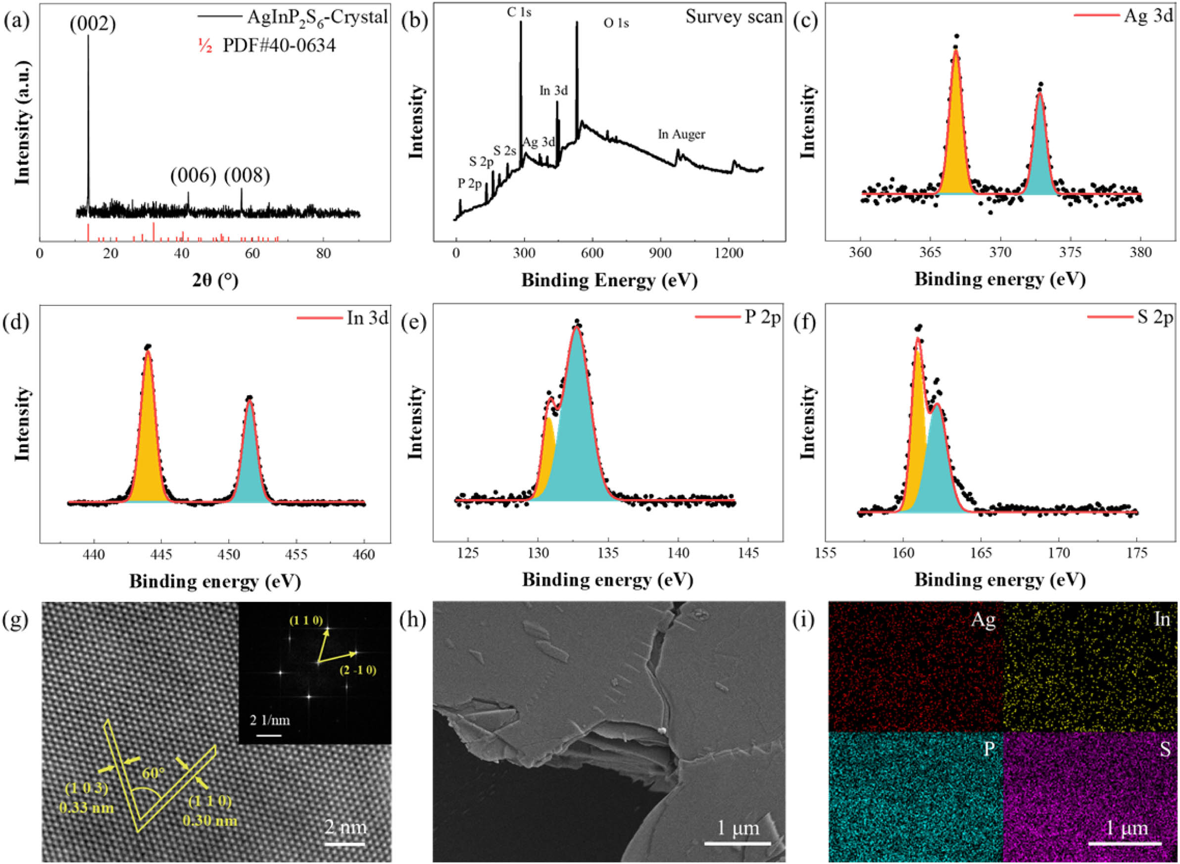
The crystal was synthesized in a two-zone furnace using CVT and exhibited a bright yellowish-brown color. The crystal structure was characterized by XRD measurements, as shown in Fig. 1(a). A set of sharp diffraction peaks was observed in the XRD pattern, with a strong peak at 13.71° attributed to the (002) facet, and two weak peaks at 41.89° and 56.93° attributed to the (006) and (008) facets, respectively, which are in good agreement with the simulated one from the crystal structure of PDF#40-0634 with the space group. The intensity of the () peak and the disappearance of other diffraction peaks indicate that the sample is in the nanocrystalline form and mainly crystallizes along the c-axis. The complete XPS spectrum shown in Fig. 1(b) indicates the presence of Ag, In, P, and S, in addition to the ubiquitous C and O elements, confirming the synthesis of the crystal. Figures 1(c)–1(f) illustrate the binding energy and verify the high quality of . Ag elements generate peaks at 366.81 eV and 372.80 eV, and the main peaks of In are located at 444.00 eV and 451.53 eV, respectively. The split-peak fitting shows that the two peaks of P atoms correspond to 130.76 and 132.75 eV, while the two peaks of S atoms correspond to 160.91 and 162.19 eV, respectively. The binding energies of the atoms were consistent with those reported in the literature [51]. The HRTEM images and corresponding selected-area electron diffraction (SAED) patterns provide a comprehensive study of the microstructure. Figure 1(g) shows well-defined lattice fringes with a face-to-face spacing of 0.30 nm and 0.33 nm, corresponding to the (110) and (103) face of , respectively, with an interfacial angle of 60°. The SAED reveals an ordered array of spots [Fig. 1(g), inset], confirming the single crystal nature of the . As shown in Fig. 1(h), the SEM images show that the sample has a clear layered structure. Energy dispersive spectroscopy (EDS) results are illustrated in Fig. 1(i), demonstrating a uniform spatial distribution of Ag, In, P, and S, which can better reflect the elemental distribution of the entire crystal owing to the relatively large depth of EDS susceptibility.
Figure 1.(a) Typical XRD pattern of crystal. (b) XPS survey scan and (c) Ag 3d, (d) In 3d, (e) P 2p, and (f) S 2p region of . Black dots and red solid lines represent experimental and fitting results, respectively. (g) TEM image of . The top-right inset is the SAED. (h) SEM image and (i) EDS results of .
As shown in Fig. 2(a), we prepared six flakes (labeled S1–S6) with thicknesses of 11.14, 21.15, 23.76, 29.29, 102.95, and 443.74 nm using the ME technique. Raman spectra were obtained with 532 nm continuous-wave (CW) laser at room temperature to study the structure and vibrational modes. As can be seen in Fig. 2(b), the Raman peaks are located at 182.08, 253.41, 374.74, and corresponding to the S-P-P, S-P-S, P-P, and P-S modes. The Raman modes in the high-frequency region () are mainly attributed to the internal vibrations of the unit, whereas the Raman spectra in the low-frequency part () are mainly affected by the vibrations of the metal atoms. The Raman signals are significantly enhanced with increasing sample thickness, but we did not observe any significant frequency shifts in the Raman modes, which may be attributed to the weak interlayer interactions.
Figure 2.(a) Optical image of flakes with different thicknesses exfoliated on a quartz substrate. (b) Room temperature Raman spectra obtained under 532 nm CW laser excitation. (c) UV-visible absorption spectra of flakes. (d) Tauc plots and the optical bandgap of flakes with different thicknesses.
The UV-visible absorption spectra measured by MStarter ABS system [52,53] are given in Fig. 2(c), which shows a gradual increase with decreasing wavelength. This demonstrates that has significant application potential in UV-visible photodetectors. As shown in Fig. 2(d) and the inset, we used the Tauc plot method to calculate the energy band structure of the flakes, and the optical bandgap was determined to be 2.57, 2.41, 2.37, 2.28, 2.11, and 2.00 eV, respectively. With an increase in the sample thickness, the bandgap decreases gradually, which shows a strong quantum constraint effect in the transverse direction. A large bandgap can effectively reduce the intrinsic ionization effect caused by thermal radiation and resist environmental thermal perturbations [49].
The band structure and bandgap parameters of were calculated using the DFT approach [54] in the first-principles method, which helps us understand the qualitative aspects of the electronic properties, showing the indirect bandgap in both the few-layer and bulk samples. In the DFT method part, we adopted the GGA-PBE functional [55] and the plane-wave basis function under the generalized gradient approximation [56]. The calculation process uses the quasi-Newton method and dispersion correction [57] to optimize the structure and then the self-consistent wave function is calculated. The K points in all the calculations were unified as . Finally, we used the complex energy band correction algorithm [58] for ultrathick energy bands (100 and 400 nm). The results are shown in Figs. 3(a)–3(d). The indirect bandgap of the monolayer sample is 2.1 eV, and the conduction band minima and valence band maxima are located at the Γ and K points in the two-dimensional Brillouin zone, respectively. The calculations in Fig. 3(e) indicate that the indirect bandgap decreases to 1.29 eV as the thickness increases to 400 nm. Although the DFT calculations usually underestimate the bandgap, this trend agrees well with the Tauc plots experimental results.
Figure 3.Theoretical band structure of (a) monolayer, (b) 10 nm, (c) 100 nm, and (d) 400 nm . (e) Theoretical bandgap as a function of thickness.
Figure 4(a) shows the μ-Z/I-scan setup used for the nonlinear optical activity experiment of small size samples. The excitation laser source is a 380 fs pulse at 1040 nm and its second harmonic at 520 nm, with a pulse repetition rate of 1 kHz. The incident laser energy is changed by a motorized attenuation filter and focused through a objective lens, with beam waists of μ and μ at the focus of the 520 nm and 1040 nm, respectively. The sample is placed on a motorized translation stage that moves in and out of the focal region from to μ. We utilize a objective lens to collect the signal light, and the nonlinear optical response of the sample is recorded by measuring the intensity change of the laser using detectors PD0, PD1, and PD2, with a small aperture diaphragm placed in front of PD2 to partially block the transmitted signal. To ensure precise targeting during the measurement, the focal position is visualized using a white light source and a CCD camera.
Figure 4.(a) Schematic of the μ-Z/I-scan setup used for the nonlinear optical activities experiment. (b) Open-aperture and (d) closed-aperture Z-scan results of the 443.74 nm flake at 520 nm femtosecond pulse. (c) Open-aperture and (e) closed-aperture Z-scan results of 443.74 nm flake at 1040 nm femtosecond pulse.
The third-order nonlinear optical properties of 443.74 nm were studied using μ-Z-scan technique, and previous studies demonstrated the reliability of this setup by testing InSe flakes [59]. Figures 4(b) and 4(c) illustrate the open-aperture Z-scan results of the 443.74 nm flakes under excitation at 520 and 1040 nm, respectively. The data points represent the experimental results, and the solid lines represent the fitting results. Note that we did not observe any obvious nonlinear optical signal from the substrate, and these responses come solely from the . The sample’s transmittance decreases as it approaches the focal point; that is, the higher the excitation energy, the lower the transmittance is. The valley value reduced from at to at , and at to at under 520 nm and 1040 nm excitation, respectively, and the shorter wavelength has larger optical absorption effect, which is in good agreement with the linear absorption spectra. We did not observe any nonlinear signals from the blank substrate, implying that the nonlinear absorption originated from . The order of the nonlinear optical response can be identified by the dependence of the normalized transmittance on the incident laser intensity . The equation of dependence is as follows [60,61]: where the slope represents the nonlinear response order, for example, for TPA, for three-photon absorption, and so on; is a constant. After fitting the open-aperture Z-scan results (Fig. 5), we conclude that the slopes of are close to 1 for both 520 and 1040 nm, indicating that the nonlinear absorption of the sample is degenerate TPA [62].
Figure 5.Relationship graphs between and of 443.74 nm flake under the excitation of (a)–(c) 520 nm and (d)–(f) 1040 nm femtosecond pulses.
Different from nonlinear absorption, as shown in Figs. 4(d) and 4(e), the closed-aperture Z-scan exhibits two different shapes, which have been divided by the corresponding open-aperture results to remove the influence of nonlinear optics absorption. The normalized transmittance presents a valley followed by a peak when the sample is scanned along the laser propagation direction at 520 nm, indicating a self-focusing effect, whereas a peak followed by a valley under excitation of 1040 nm indicates a self-defocusing effect. We derive the nonlinear absorption coefficients and nonlinear refractive index obtained from the open- and closed-aperture Z-scan results using the analytical solution of the Z-scan curves, respectively [63,64]. Because the linear absorption can be neglected [65,66], the real and imaginary parts of the third-order nonlinear optical susceptibility and can be further derived from and , where and are the velocity and wavelength of incident laser, and is the refractive index. We can use the figure of merit (FOM) to eliminate the differences in nonlinear magnetization caused by different linear absorption coefficients, which can be calculated from and , where is the linear absorption coefficient. These parameters are all summarized in Table 1.
Linear and Nonlinear Optical Parameters of the 443.74 nm AgInP2S6 Flake
Thickness (nm)
Laser (nm)
()
(cm/GW)
(esu)
(esu cm)
()
(esu)
(esu cm)
443.74
520
8098.79
21.33
1040
1753.39
1.21
Figure 6.μ-I-scan results of the flakes under the excitation of (a) 520 nm and (b) 1040 nm femtosecond pulses, respectively.
To further investigate the nonlinear absorption mechanism and ultrafast carrier dynamics of the flakes, non-degenerate time-resolved reflection μ-pump-probe measurements were performed with a pump laser at 520 nm and a probe laser at 1040 nm [Fig. 7(a)]. The laser source is generated by a femtosecond laser with the center wavelength of 1040 nm, pulse width of 380 fs, and pulse repetition rate of 100 kHz. The incident laser is divided into two parts by a beam splitter, one of which is a 1040 nm laser for probe light, and the other is doubled to 520 nm by a BBO crystal as a pump light. We set a time delay between the pump light and the probe light by a retroreflector located on the motorized translation stage in the pump light path. It is defined as the zero-delay position when the pump and probe light pulses reach the sample position at the same time. The two beams are focused through a 50× objective lens, and the signal reflected from the sample is collected by detector PD1, where the pump light is filtered out by a 532 nm long-pass filter. Similarly, to ensure that the pump and probe beams are accurately focused at the same position, the focal position from the opposite side of the sample is visualized using a white light source and a CCD camera.
Figure 7.(a) Schematic of the μ-pump-probe setup used for the ultrafast carrier dynamics experiment. Carrier relaxation process with different pump intensities of the (b) 443.74 nm and (c) 102.95 nm flakes. The insets shows versus the pump intensity at zero-time delay. (d) Excitation intensity-dependent PL spectra of 443.74 nm obtained under CW laser excitation at 532 nm. (e) Maximum PL intensity as a function of excitation intensity.
The non-degenerate pump-probe results of the 443.74 and 102.95 nm flakes are shown in Figs. 7(b) and 7(c), in which the excitation intensity of the pump laser varies from 1.07 to , and the probe laser intensity is , which is much lower than the pump laser intensity. All the samples exhibit same reflectivity variation patterns, indicating same nonlinear optical response mechanism. The ultrafast dynamic process mainly consists of three stages. (I) The differential reflectance decreases rapidly and reaches its minimum value within a few hundred femtoseconds. (II) A fast recovery of the positive occurs within a few tens of ps. (III) A slow recovery lasting over 50 ps occurs. The linear dependence of the peak on the pump intensity confirms the TPA effect of , which is consistent with our I-scan results.
The ultrafast dynamic results generally show a laser-induced absorption process followed by a slow relaxation process. The experimental data were fitted using a bi-exponential model [70,71]: where is the instantaneous absorption signal at the probe wavelength, and are the corresponding amplitudes, is the delay time, and and are the lifetimes of fast and slow excited carriers in the relaxation process, respectively.
The fitting results show that the fast relaxation time and slow relaxation time of the 443.74 nm flake are 3.9 ps and 48.66 ps, respectively, and both relaxation times increase significantly with the sample thickness decreasing to 102.95 nm, which are 61.76 ps and 61.60 ps, respectively. This fast time constant proves that the photoexcited carriers may undergo an intra-defect-band relaxation process [51]. PL spectroscopy was performed with a 532 nm CW laser, as shown in Fig. 7(d), and a wide asymmetric peak centered at can be observed in all the PL spectra, which is related to deep-level defects [72]. The PL emission intensity varies with the excitation intensity; however, the PL emission peak does not change. We conclude that the wideband emission at may be due to the radiative recombination of non-equilibrium carriers in the localized defect state. As illustrated in Fig. 7(e), the PL emission intensity increases sublinearly with the excitation intensity and becomes saturated at high excitation intensities, a typical feature of defect-assisted emission [73]. Under laser excitation, valence band electrons absorb photons, transition to the conduction band, and then relax to the bottom of the conduction band. Some of the carriers recombine in a non-radiative recombination mode, while the rest undergo radiative recombination through the defect level.
3. CONCLUSION
In summary, a comprehensive analysis of the nonlinear optical activity of was performed. flakes with different thicknesses were prepared by CVT and ME and characterized by XRD, SEM, HRTEM, XPS, and Raman spectroscopy. μ-Z/I-scan measurements show that has a TPA response both under 520 and 1040 nm femtosecond laser excitation. The sample exhibited self-focusing and self-defocusing under excitation at 520 and 1040 nm, respectively. The TPA coefficient of the flakes decreased with increasing thickness, whereas the TPA saturation intensity exhibited the opposite behavior. The TPA coefficient under 520 nm excitation is an order of magnitude larger than that under 1040 nm excitation, while the saturation intensity at 520 nm is an order of magnitude smaller than that at 1040 nm, indicating that the flakes are more likely to be saturated in the visible range. In addition, ultrafast carrier dynamics and PL spectroscopy revealed that the flakes first exhibited laser-induced absorption, followed by carrier relaxation processes, including non-radiative and defect-level-assisted recombination processes. Detailed characterizations of the linear and nonlinear optical aspects and ultrafast carrier dynamics are conducive to the important application of in optoelectronic devices.
[28] M. C. Friedel. Soufre et ses composés—sur une nouvelle série de sulfophosphures, les thiohypophosphates. C. R. l’Academie. Sci. Ser. III, 119, 260(1894).
[29] L. Ferrand. Bull. Soc. Chie. Fr., 13, 115(1895).
 AI Video Guide
  AI Picture Guide
 AI One Sentence