• Acta Optica Sinica
  • Vol. 43, Issue 21, 2124001 (2023)
Chunfang Wu1、*, Yan Zhang1, Hao Pan1, Yechuan Zhu1, Zhanjun Yang2, and Jie Wei3
Author Affiliations
  • 1School of Opto-Electronical Engineering, Xi'an Technological University, Xi'an 710021, Shaanxi , China
  • 2Northwest Branch, China Datang Corporation Science and Technology General Research Institute Co., Ltd., Xi'an 710018, Shaanxi , China
  • 3School of Electronic Science and Engineering, Xi'an Jiaotong University, Xi'an 710049, Shaanxi , China
  • show less
    DOI: 10.3788/AOS230867 Cite this Article Set citation alerts
    Chunfang Wu, Yan Zhang, Hao Pan, Yechuan Zhu, Zhanjun Yang, Jie Wei. Design, Preparation, and Properties of Gold Grating/Nanoparticles SERS Substrate[J]. Acta Optica Sinica, 2023, 43(21): 2124001 Copy Citation Text show less
    Schematic of the substrate for FDTD simulation. (a) Grating; (b) grating/nanoparticles; (c) unit cross-section for FDTD simulation
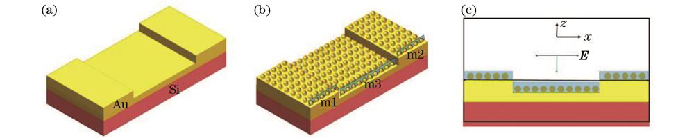
    Fig. 1. Schematic of the substrate for FDTD simulation. (a) Grating; (b) grating/nanoparticles; (c) unit cross-section for FDTD simulation
    Simulated reflectance spectra. (a) Au gratings with varied periodicities; (b) Au nanoparticles array with diameter of 25 nm, Au gratings with 580-nm periodicity, corresponding Au grating/ nanosparticles hybrid structure
    Fig. 2. Simulated reflectance spectra. (a) Au gratings with varied periodicities; (b) Au nanoparticles array with diameter of 25 nm, Au gratings with 580-nm periodicity, corresponding Au grating/ nanosparticles hybrid structure
    Simulated electric field distribution around particles. (a) On the surface of grating groove; (b) on the surface of Si wafer; (c) on the surface of left grating ridge; (d) on the surface of right grating ridge
    Fig. 3. Simulated electric field distribution around particles. (a) On the surface of grating groove; (b) on the surface of Si wafer; (c) on the surface of left grating ridge; (d) on the surface of right grating ridge
    Schematic of Au grating preparation
    Fig. 4. Schematic of Au grating preparation
    Au nanoparticles. (a) TEM image; (b) diameter distribution histogram
    Fig. 5. Au nanoparticles. (a) TEM image; (b) diameter distribution histogram
    Au grating. (a) AFM false-color height image; (b) surface profile
    Fig. 6. Au grating. (a) AFM false-color height image; (b) surface profile
    SEM images. (a) Au grating under low magnification, inset is photograph of the grating taken at different angles; (b) Au grating under high magnification; (c) Au grating/nanoparticles hybrid structure
    Fig. 7. SEM images. (a) Au grating under low magnification, inset is photograph of the grating taken at different angles; (b) Au grating under high magnification; (c) Au grating/nanoparticles hybrid structure
    Reflectance spectra of Au nanoparticles on Si wafer, Au grating, and Au grating/nanoparticles hybrid structure
    Fig. 8. Reflectance spectra of Au nanoparticles on Si wafer, Au grating, and Au grating/nanoparticles hybrid structure
    SERS spectra of R6G solution with different concentrations collected on different substrates. (a) Au grating/nanoparticles hybrid substrate; (b) common substrate formed by Au nanoparticles distribution on silicon wafers
    Fig. 9. SERS spectra of R6G solution with different concentrations collected on different substrates. (a) Au grating/nanoparticles hybrid substrate; (b) common substrate formed by Au nanoparticles distribution on silicon wafers
    SERS spectra of R6G with different concentrations on Si wafer, Au nanoparticles substrate, and Au grating/nanoparticles hybrid substrate
    Fig. 10. SERS spectra of R6G with different concentrations on Si wafer, Au nanoparticles substrate, and Au grating/nanoparticles hybrid substrate
    SERS mapping on Au grating/nanoparticles hybrid substrate. (a) mapping image by monitoring the intensity of the Raman peak at 614 cm-1; (b) RSD comparsion of SERS intensity for peak at 614 cm-1, 1365 cm-1,and 1512 cm-1
    Fig. 11. SERS mapping on Au grating/nanoparticles hybrid substrate. (a) mapping image by monitoring the intensity of the Raman peak at 614 cm-1; (b) RSD comparsion of SERS intensity for peak at 614 cm-1, 1365 cm-1,and 1512 cm-1
    Chunfang Wu, Yan Zhang, Hao Pan, Yechuan Zhu, Zhanjun Yang, Jie Wei. Design, Preparation, and Properties of Gold Grating/Nanoparticles SERS Substrate[J]. Acta Optica Sinica, 2023, 43(21): 2124001
    Download Citation