
Lei Chen, Han Ye, Yumin Liu, Dong Wu, Rui Ma, Zhongyuan Yu. Numerical investigations of an optical switch based on silicon stripe waveguide embedded with vanadium dioxide layers[J]. Photonics Research, 2017, 5(4): 335
- Photonics Research
- Vol. 5, Issue 4, 335 (2017)
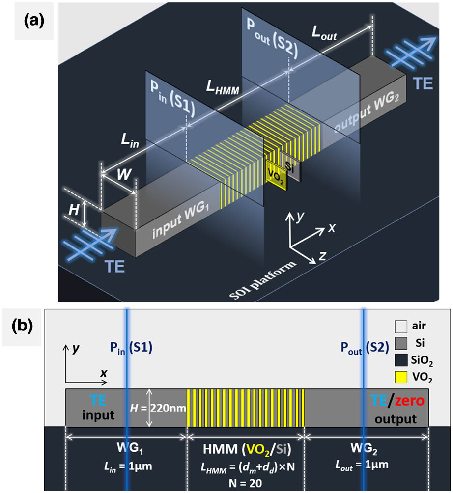
Fig. 1. (a) 3D and (b) lateral view of the proposed optical switch inserted with an HMM structure consisting of 20-pair alternating VO 2 / Si
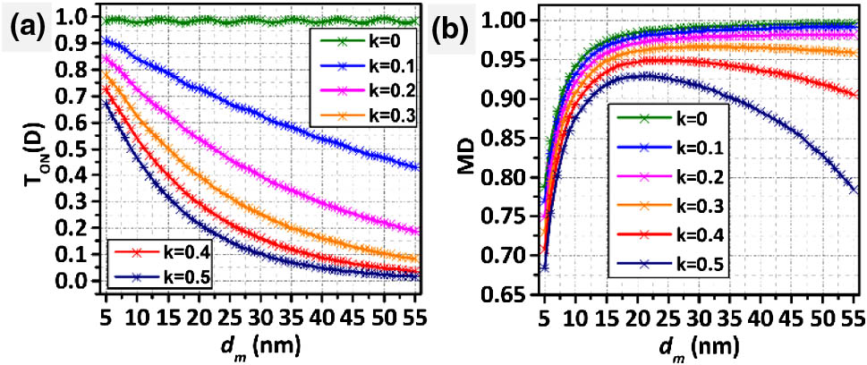
Fig. 2. (a) Transmittance diagram of T ON VO 2 k n ˜ exp ( D ) VO 2 n ˜ exp ( D ) = 3.1309 + 0.3612 i d m VO 2 k n ˜ exp ( M )
Fig. 3. Electric field distribution of TE mode propagation for (a) “ON” and (b) “OFF” state with zoom-in views of the HMM structure.
Fig. 4. Power flux density Poavx distribution of TE mode propagation for (a) “ON” and (b) “OFF” state with zoom-in views of the HMM structure.
Fig. 5. Transmission diagram of (a) T ON D T OFF M d m
Fig. 6. Electric field intensity distribution in an optical switch in“OFF” state with different HMM length of (a) L HMM = 200 nm d m = d d = 5 L HMM = 600 nm d m = d d = 15
Fig. 7. Calculated (a) MD and (b) IL as a function of wavelength with d m L HMM
Fig. 8. Based on an optical switch using W-doped VO 2 d m = 5 nm n k n ˜ exp ( M )

Set citation alerts for the article
Please enter your email address
© Copyright 2018-2021 | Chinese Laser Press. All Rights Reserved 沪ICP备15018463号-20