Abstract
A novel scheme for the design of an ultra-compact and high-performance optical switch is proposed and investigated numerically. Based on a standard silicon (Si) photonic stripe waveguide, a section of hyperbolic metamaterials (HMM) consisting of 20-pair alternating vanadium dioxide thin layers is inserted to realize the switching of fundamental TE mode propagation. Finite-element-method simulation results show that, with the help of an HMM with a size of (), the ON/OFF switching for fundamental TE mode propagation in an Si waveguide can be characterized by modulation depth (MD) of 5.6 dB and insertion loss (IL) of 1.25 dB. It also allows for a relatively wide operating bandwidth of 215 nm maintaining and . Furthermore, we discuss that the tungsten-doped layers could be useful for reducing metal-insulator-transition temperature and thus improving switching performance. In general, our findings may provide some useful ideas for optical switch design and application in an on-chip all-optical communication system with a demanding integration level.1. INTRODUCTION
Recent years have seen promising development of photonic devices that are based on a great variety of functional micro-/nano-structures and conventional or alternative plasmonic materials, which include optical interconnects, modulators, detectors, splitters, switches, mode converters, lasers, and so on [1–7]. Among them, it is still a challenge for the full implementation of all-optical switches because they are always expected to feature milliwatt power consumption, picosecond switching time, and tenth-decibel insertion loss (IL). In addition, we also characterize all-optical switches with high compactness and large modulation depth (MD) in an on-chip optical communication system [8]. Researchers have performed numerous numerical and experimental work on switch design utilizing the resonance cavity effect [5], optical interference [9], phase-change property [10], light saturation absorption [11,12], and so on. As we all know, in the near-infrared region, conventional metals (e.g., gold, silver, copper, and aluminum) are extensively used in photonic devices due to their good plasmonic behavior and low optical loss, despite the fact that they have low melting temperature, relative softness, and metal contamination to surrounding mediums in the form of ion diffusion [13]. Nevertheless, the promising alternative plasmonic materials have greatly surprised us because of the tunable optical property, CMOS-compatibility, chemical stability, and high-temperature durability [14]. They could be, for example, transition metal nitrides (e.g., titanium nitride, zirconium nitride, hafnium nitride), transparent conducting oxides (e.g., indium-tin-oxide, aluminum-doped zinc oxide, germanium-doped zinc oxide), phase-change materials [e.g., vanadium dioxide ()], 2D materials (e.g., graphene, hexagonal boron nitride), or high-doping semiconductors (e.g., silicon, germanium) [14–18]. Furthermore, these plasmonic materials are widely used in combination with specific dielectrics. Specifically, we can use gold/silver combined with alumina in ultraviolent region, gold/silver combined with titanium oxides in visible region, titanium nitride/indium tin oxides combined with silicon or silicon dioxide in near-infrared region, and indium-gallium-arsenide/graphene combined with alumina in mid-infrared even terahertz regions [19].
Material of is essential for applications in all-optical computing, optical communication, and smart laser shielding for military use. Among a series of vanadium oxides with variable valence (e.g., , ), the distinct feature of is the reversible metal-to-insulator transition (MIT) behavior at a critical temperature of about (68°C), which brings in sharp optical contrast from high transmittance to reflectance with greatly varied permittivity for a near-infrared light wave [20]. This is because, with room temperature approaching to , the lattice structure of a film will change from monoclinic insulating phase to a tetragonal metallic phase, which causes its electrical conductivity increased by several orders of magnitudes. The optical property of film can be tuned thermally, electrically, magnetically, and by strain [21]. Furthermore, we could probably promote electrical and optical properties of by manipulating its . The tunability significantly facilitates the development of room-temperature infrared detection and optical switching.
In this paper, to remove complex and bulky structures, we propose that the silicon photonic (Si) waveguide inserted with a section of hyperbolic material (HMM) can be exploited as an optical switch. On the one hand, HMM is an artificial structure with manageable electromagnetic properties that cannot be obtained from conventional structures. Merely the most basic structure consisting of alternating metal/insulator layers can induce a strong absorption effect or become transparent to an incoming light wave [22]. On the other hand, the HMM structure greatly contributes to complete light–matter interaction. Therefore, propagation of the dominant TE mode in the Si stripe waveguide can be controlled by a well-designed HMM. The designed structure can achieve ON/OFF switching function after laser irradiation [23]. Alternatively, the layers also can be extended to contact with metal electrodes for active electric control. To the best of our knowledge, the proposed optical switch has been neither studied nor previously reported.
Sign up for Photonics Research TOC. Get the latest issue of Photonics Research delivered right to you!Sign up now
2. NUMERICAL SIMULATION
A. Design and Modeling
Figure 1 shows a schematic view of the proposed optical switch without keeping the geometry ratio. With embedded layers, the Si stripe waveguide (WG) has a standard cross-section of , with length of . It can be divided into three parts: input with , HMM structure with , and output with . The parameters of , , and indicate the length of a layer, length of a Si layer, and number of pairs, respectively. Considering device compactness, we vary the values of and from 5 to 55 nm, and set . Performed in the wave-optics module of COMSOL Multiphysics software, finite-element-method boundary mode analysis combined with perfectly matched layers is used to solve the 2D model, as shown in Fig. 1(b). Numerical port is set to launch the dominant fundamental TE mode. For the accuracy and convergence of simulation results, we discretize the device structure using high-quality mapping mesh and boundary layer.
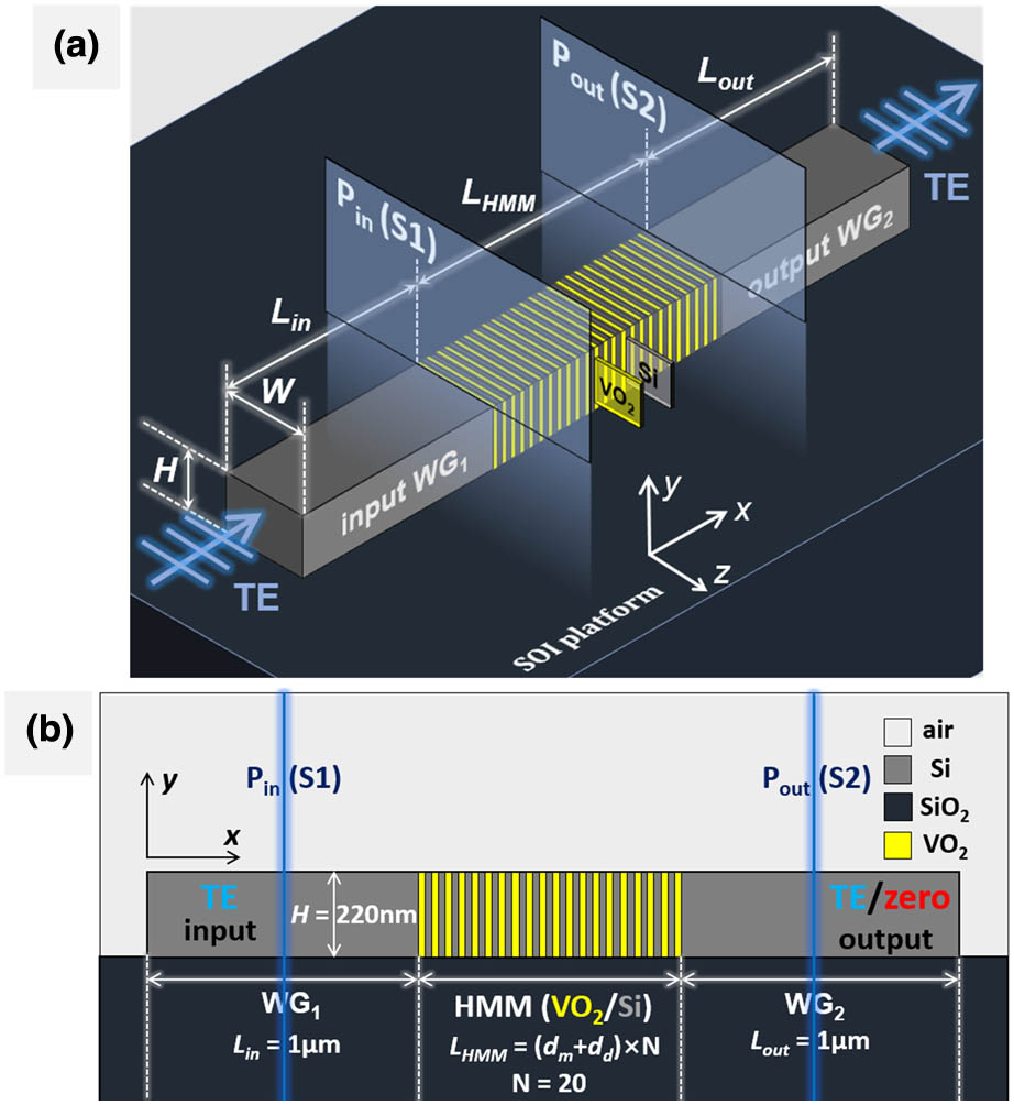
Figure 1.(a) 3D and (b) lateral view of the proposed optical switch inserted with an HMM structure consisting of 20-pair alternating layers on a glass substrate.
The refractive indices of Si, , and air are set as 3.48, 1.45, and 1, respectively [24]. Here we use experimental refractive index () of for the metallic after MIT process and for dielectric in normal state [25]. Based on the effective medium method [26,27], we can consider the 20-pair layers as a section of HMM, with optical property characterized by the effective tensor parallel {} and perpendicular [] to the anisotropy axis ( axis in our model). The metal filling factor of is set as 0.5 for ease of control. Note that for a material, the real part indicates impedance matching, while the imaginary part indicates absorption ability.
Next, we use three performance indices to evaluate the optical switch [2,5]. We first denote the component of power flux density as Poavx. Then the optical power input/output the optical switch is calculated as the integral value of Poavx along boundary S1/S2, which is labeled as in Fig. 1(b). Accordingly, the TE mode transmittance is defined as for “ON” state and for “OFF” state. Therefore, performance indices of MD and IL can be calculated by expressions of and , respectively [5]. We also calculate the operating bandwidth (BW) that is a wavelength range maintaining . An optical switch with MD higher than 5 dB is sufficient and practicable as validated in Ref. [10].
B. Results and Discussion
We first explore how absorption losses caused by of and control the switching performance. In Fig. 2(a), for of varying from 0.0 to 0.5, all () rapidly decrease as layer length increases. Note that nearly perfect transmission efficiency can be obtained when due to good impedance matching and zero absorption loss. Furthermore, shorter HMM can cause fewer losses to the TE mode. In Fig. 2(b), the curve of MD shows a different tendency with that of () due to the great impact of on (). As a result, we can design a high-performance optical switch by following the MD index (note that the IL is not considered here).

Figure 2.(a) Transmittance diagram of based on dielectric layers with varying of . (b) Using the same dielectric layers with constant , relationship curve of MD- is calculated based on metallic layers for different of .
Then we make an intuitive presentation of the “ON”/“OFF” switching by plotting the norm electric field distribution, as shown in Fig. 3. We base the following simulation on an ultra-compact HMM with (). It can be clearly seen that, for the “ON” state, the TE mode can pass through with an undistorted field profile and slightly weakened field intensity. However, for the “OFF” state, the field intensity of TE mode is rapidly reduced. Furthermore, as shown in Fig. 4, we plot the Poavx distribution and total electromagnetic losses caused by HMM. Figure 4(a) shows the normal propagation without radiation. In the “OFF” state, it is indicated that the TE mode is effectively isolated by the HMM with little radiation power. This means a lot to the integration with other components because it could cause little crossing disturbance.
Figure 3.Electric field distribution of TE mode propagation for (a) “ON” and (b) “OFF” state with zoom-in views of the HMM structure.
Figure 4.Power flux density Poavx distribution of TE mode propagation for (a) “ON” and (b) “OFF” state with zoom-in views of the HMM structure.
Next, we explore the propagation loss mechanism of the HMM inserted Si waveguide. The losses of the TE mode can be caused by HMM-induced absorption, reflection, and radiation. Figure 5 illustrates that HMM will cause zero/little reflection to the TE mode when it operates in the “ON”/“OFF” state. Two points are worth mentioning: first, seeing that the effect of on () has been simulated in Fig. 2(a), here we use in Fig. 5(a), which is helpful in explaining the impedance matching. Regardless of the difference of refractive index between Si (3.48) and dielectric (3.1309), the switch can still perform well with a 2.2 μm long HMM. Second, the reflection curve obtained from Fig. 5(b) well explains the standing pattern in from Fig. 3(b). Furthermore, Fig. 6 gives an intuitive view of the electric field intensity distribution, which indicates that the power radiated into surrounding mediums is negligible. We therefore conclude that the propagation loss is mainly resulted from absorption. It can be explained by the effective relative permittivity of HMM. Calculation results show that the HMM structure will present an anisotropic optical property with and () when behaves as a metal. As a result, for one thing, the noticed reflection in Fig. 5(b) is due to the reduced refractive index from 3.48 to 2.4191 at the interface. For another thing, the significantly increased values of 6.06 and 16.14 are responsible for the huge absorption of the TE mode. In other words, compared with pure metal or insulator, the HMM structure consisting of alternating metal/insulator layers shows desirable optical property very dissimilar to that of either metal or insulator.
Figure 5.Transmission diagram of (a) () and (b) () for an optical switch with varying from 5 to 55 nm.
Figure 6.Electric field intensity distribution in an optical switch in“OFF” state with different HMM length of (a) ( nm) and (b) ( nm).
Last, as shown in Fig. 7, we discuss the propagation loss introduced by HMM length and calculate the device operating BW. On one hand, Fig. 7 indicates that the length of HMM structure plays a decisive role in device performance. That is, a too-long HMM structure will cause huge loss to the TE mode when the device operates either in the “ON” or “OFF” state. On the other hand, the device can achieve a wide operating BW of 215 nm with while maintaining a constant IL of 1.25 dB. Therefore, considering the balance between MD and IL, an optical switch characterized by an ultra-compact footprint of (), moderate MD of 5.6 dB, and IL of 1.25 dB is our first choice.
Figure 7.Calculated (a) MD and (b) IL as a function of wavelength with () varying from 5 nm (200 nm) to 55 nm (2200 nm).
3. SWITCHING FEATURE OF DOPED VO2
Based on the experiments reported in Refs. [28,29], we know that an undoped film has MIT temperature of and temperature window of merely 1°C–2°C. However, the could be manipulated by chemical doping. For example, we could reduce utilizing doping elements of W, Mo, Nb, Ta, F, Te, Fe, etc., increase utilizing doping elements of Al, Ge, Ga, etc., and simply change utilizing doping elements of Cu and Ti. Making continuous optical modulation a reality, tungsten (W)-doped thin film works best. This is because it achieves not only a reduced , but also a relatively wide temperature window. We can also expect to obtain the following advantages. First, the switching time could be largely improved because of the doping percent influenced electrical conductivity. Second, the W-doped could get its absorbing ability promoted during MIT process. Third, the reduced could protect the Si waveguide and other components from laser damage, because the time of MIT process is greatly shortend. In general, a relatively low is beneficial for optical switching performance. To simulate the effect of doping-induced complex refractive index variation on device performance, MD is calculated as a function of real part and imaginary part of . It is worth noting that there is no accurate relationship between complex refractive index and chemical doping percent so far. Therefore, Fig. 8 indicates a possibility of improving the switching performance.
Figure 8.Based on an optical switch using W-doped layers (), MD varies as a function of both and of .
4. EXPERIMENTAL FEASIBILITY
With support from some reported experimental work [28–30], we discuss the practicable experimental processes despite the fact that our design is based on numerical simulations. First, on the silicon-on-insulator (SOI) platform, the WG and Si layers in HMM can be written using electron beam lithography (EBL). Second, layers in HMM can be directly prepared on Si waveguide using pulsed laser deposition. Finally, shaping the device with required dimension can be realized using EBL again. In addition, the element of W can be doped in film co-sputtering a W wire during the film deposition process [28].
5. CONCLUSION
In summary, we numerically demonstrate an ultra-compact silicon waveguide-based optical switch utilizing a multilayer hyperbolic metamaterial. Under laser irradiation, the Si waveguide inserted with an HMM with size of () could offer good ON/OFF switching performance with MD of 5.6 dB, low IL of 1.25 dB, and operating BW of 215 nm. Furthermore, the SOI-based simple and compact device structure makes it easy to cooperate with other components in an on-chip integrated circuit. We also can dope the layer with a variety of elements to realize continuous modulation of its optical property. In general, our findings may provide some useful ideas for optical switch design and application in an on-chip all-optical communication system with demanding integration level.
References
[1] C. Wan, T. K. Gaylord, M. S. Bakir. Grating design for interlayer optical interconnection of in-plane waveguides. Appl. Opt., 55, 2601-2610(2016).
[2] G. T. Reed, G. Mashanovich, F. Y. Gardes, D. J. Thomson. Silicon optical modulators. Nat. Photonics, 4, 518-526(2010).
[3] J. Wang, Z. Cheng, Z. Chen, X. Wan, B. Zhu, H. K. Tsang, C. Shu, J. Xu. High-responsivity graphene-on-silicon slot waveguide photodetectors. Nanoscale, 8, 13206-13211(2016).
[4] K. Wen, Y. Hu, L. Chen, J. Zhou, L. Lei, Z. Guo. Design of an optical power and wavelength splitter based on subwavelength waveguides. J. Lightwave Technol., 32, 3020-3026(2014).
[5] P. Dastmalchi, G. Veronis. Plasmonic switches based on subwavelength cavity resonators. J. Opt. Soc. Am. B, 33, 2486-2492(2016).
[6] J. Kim, S. Y. Lee, H. Park, K. Lee, B. Lee. Reflectionless compact plasmonic waveguide mode converter by using a mode-selective cavity. Opt. Express, 23, 9004-9013(2015).
[7] Y. Li, W. P. Huang. Electrically-pumped plasmonic lasers based on low-loss hybrid SPP waveguide. Opt. Express, 23, 24843-24849(2015).
[8] A. Emboras, C. Hoessbacher, C. Haffner, W. Heni, U. Koch, P. Ma, Y. Fedoryshyn, J. Niegemann, C. Hafner, J. Leuthold. Electrically controlled plasmonic switches and modulators. IEEE J. Sel. Top. Quantum Electron., 21, 276-283(2015).
[9] P. P. Sahu. Theoretical investigation of all optical switch based on compact surface plasmonic two mode interference coupler. J. Lightwave Technol., 34, 1300-1305(2016).
[10] B. Gholipour, J. Zhang, K. F. MacDonald, D. W. Hewak, N. I. Zheludev. An all-optical, non-volatile, bidirectional, phase-change meta-switch. Adv. Mater., 25, 3050-3054(2013).
[11] J. Li, J. Tao, Z. H. Chen, X. G. Huang. All-optical controlling based on nonlinear graphene plasmonic waveguides. Opt. Express, 24, 22169-22176(2016).
[12] G. X. Ni, L. Wang, M. D. Goldflam, M. Wagner, Z. Fei, A. S. McLeod, M. K. Liu, F. Keilmann, B. Özyilmaz, A. H. C. Neto, J. Hone, M. M. Fogler, D. N. Basov. Ultrafast optical switching of infrared plasmon polaritons in high-mobility graphene. Nat. Photonics, 10, 244-247(2016).
[13] G. V. Naik, V. M. Shalaev, A. Boltasseva. Alternative plasmonic materials: beyond gold and silver. Adv. Mater., 25, 3264-3294(2013).
[14] G. V. Naik, J. Kim, A. Boltasseva. Oxides and nitrides as alternative plasmonic materials in the optical range. Opt. Express, 1, 1090-1099(2011).
[15] A. Lalisse, G. Tessier, J. Plain, G. Baffou. Plasmonic efficiencies of nanoparticles made of metal nitrides (TiN, ZrN) compared with gold. Sci. Rep., 6, 38647(2016).
[16] V. E. Babicheva, A. Boltasseva, A. V. Lavrinenko. Transparent conducting oxides for electro-optical plasmonic modulators. Nanophotonics, 4, 165-185(2015).
[17] C. T. Riley, J. S. T. Smalley, K. W. Post, D. N. Basov, Y. Fainman, D. Wang, Z. Liu, D. J. Sirbuly. High-quality, ultraconformal aluminum-doped zinc oxide nanoplasmonic and hyperbolic metamaterials. Small, 12, 892-901(2016).
[18] R. Alaee, M. Albooyeh, S. Tretyakov, C. Rockstuhl. Phase-change material-based nanoantennas with tunable radiation patterns. Opt. Lett., 41, 4099-4102(2016).
[19] P. Shekhar, J. Atkinson, Z. Jacob. Hyperbolic metamaterials: fundamentals and applications. Nano Convergence, 1, 14(2014).
[20] J. H. Choe, J. T. Kim. Design of vanadium oxide-based plasmonic modulator for both TE and TM modes. IEEE Photon. Technol. Lett., 27, 514-517(2015).
[21] S. B. Choi, J. S. Kyoung, H. S. Kim, H. R. Park, B. J. Kim, Y. H. Ahn, F. Rotermund, H. T. Kim, K. J. Ahn, D. S. Kim. Nanopattern enabled terahertz all-optical switching on vanadium dioxide thin film. Appl. Phys. Lett., 98, 071105(2011).
[22] A. Poddubny, I. Iorsh, P. Belov, Y. Kivshar. Hyperbolic metamaterials. Nat. Photonics, 7, 948-957(2013).
[23] D. W. Ferrara, E. R. MacQuarrie, V. D. B. J. Nag, A. B. Kaye, R. F. H. Jr. Plasmonic enhancement of the vanadium dioxide phase transition induced by low-power laser irradiation. Appl. Phys. A, 108, 255-261(2012).
[24] L. Chen, Y. Liu, Z. Yu, D. Wu, R. Ma, Y. Zhang, H. Ye. Numerical investigations of a near-infrared plasmonic refractive index sensor with extremely high figure of merit and low loss based on the hybrid plasmonic waveguide-nanocavity system. Opt. Express, 24, 23260-23270(2016).
[25] M. Kim, J. Jeong, J. K. S. Poon, G. V. Eleftheriades. Vanadium-dioxide-assisted digital optical metasurfaces for dynamic wavefront engineering. J. Opt. Soc. Am. B, 33, 980-988(2016).
[26] T. Li, J. B. Khurgin. Hyperbolic metamaterials: beyond the effective medium theory. Optica, 3, 1388-1396(2016).
[27] V. E. Babicheva, M. Y. Shalaginov, S. Ishii, A. Boltasseva, A. V. Kildishev. Finite-width plasmonic waveguides with hyperbolic multilayer cladding. Opt. Express, 23, 9681(2015).
[28] G. K. Bebek, M. N. F. Hoqie, M. Holtz, Z. Fan, A. A. Bernussi. Continuous tuning of W-doped VO2 optical properties for terahertz analog applications. Appl. Phys. Lett., 105, 201902(2014).
[29] T. Wang, H. Yu, X. Dong, Y. D. Jiang, R. L. Hu. Modeling and experiments of N-doped vanadium oxide prepared by a reactive sputtering process. Chin. Phys. B, 24, 038102(2015).
[30] R. M. Briggs, I. M. Pryce, H. A. Atwater. Compact silicon photonic waveguide modulator based on the vanadium dioxide metal-insulator phase transition. Opt. Express, 18, 11192-11201(2010).


