
Honggang Chen, Bo Zhang, Weidong Ma, Yi Hu, Xuerui Liang, Leilei Hu, Feng Li, Lan Ding. Automatic Bias Volatge Control Technology of In-Phase Quadrature-Phase Silicon-Based Optical Modulator[J]. Acta Optica Sinica, 2019, 39(3): 0306003
- Acta Optica Sinica
- Vol. 39, Issue 3, 0306003 (2019)
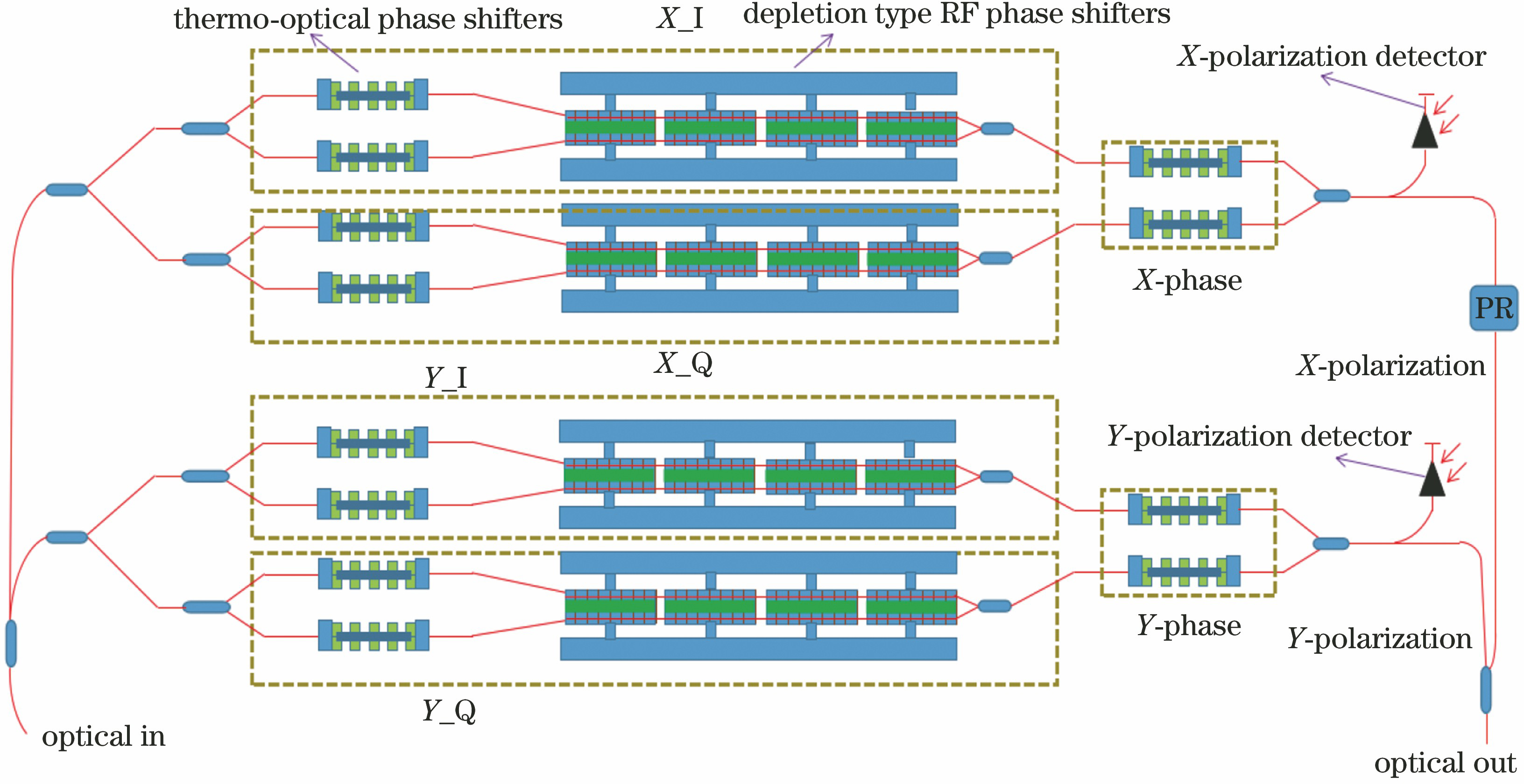
Fig. 1. Model diagram of DPMZ IQ silicon-based optical modulator
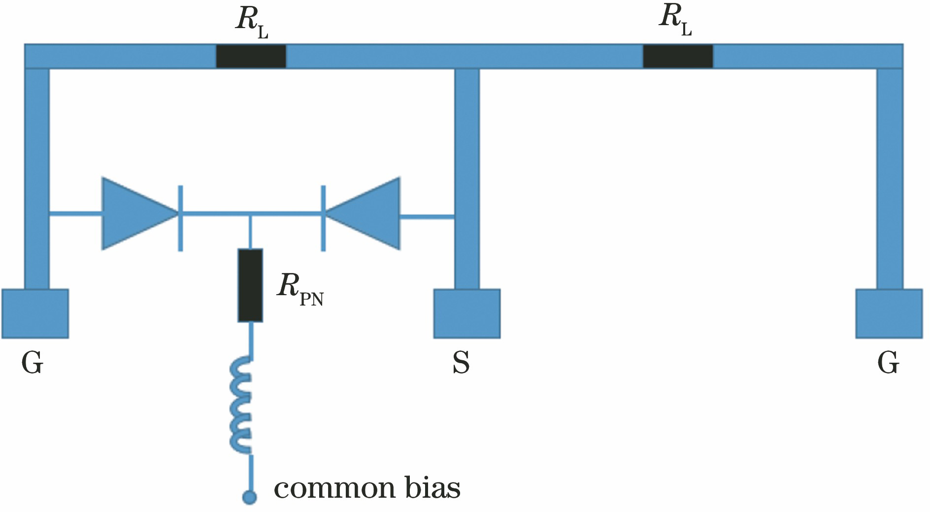
Fig. 2. Equivalent circuit model of push-pull modulation in silicon-based optical modulator (common cathode)
Fig. 3. Bias points control flowchart of channel I, channel Q, and channel Phase. (a) Initialization search; (b) closed loop locking control
Fig. 4. Simulation results of MPD feedback signal spectra after channel I and channel Q applied different bias voltages. (a) Amplitude spectra; (b) phase spectra
Fig. 5. Simulation waveforms of MPD feedback signals at time domain after channel I and channel Q applied different bias voltages
Fig. 6. Simulation results of MPD feedback signal spectra after channel Phase applied different bias voltages. (a) Amplitude spectra at sum frequency; (b) phase spectra at sum frequency
Fig. 7. Simulation waveforms of MPD feedback signals at time domain after channel Phase applied different bias voltages
Fig. 8. Test platform for direct current bias voltage closed-loop control of IQ silicon-based optical modulator
Fig. 9. Test results of MPD feedback signal spectra after channel I and channel Q applied different bias voltages. (a) Amplitude spectra; (b) phase spectra
Fig. 10. Test waveforms of MPD feedback signals at time domain after channel I and channel Q applied different bias voltages
Fig. 11. Test results of MPD feedback signal spectra after channel Phase applied different bias voltages. (a) Amplitude spectra; (b) phase spectra
Fig. 12. Test waveforms of MPD feedback signals at time domain after channel Phase applied different bias voltages
Fig. 13. Constellation diagrams of optical signals in QPSK modulation after channel I, channel Q, and channel Phase applied different bias voltages. (a) Revised by algorithm; (b) 0.96Vπ, 1.04Vπ and 0.96Vπ/2 ; (c) 0.96Vπ, 0.96Vπ and 0.96Vπ/2; (d) 1.04Vπ, 1.04Vπ and 0.96Vπ/2; (e) 1.04Vπ, 0.96Vπ and 0.96Vπ/2; (f) 0.96Vπ, 1.04Vπ and 1.04Vπ/2; (g) 0.96Vπ, 0.96Vπ and 1.04Vπ/2; (h) 1.04Vπ, 1.04Vπ and 1.04Vπ/2 ; (i) 1.04Vπ, 0.96Vπ and 1.04Vπ/2
| ||||||||||||||||||||||
Table 1. Sine dither signal parameters
|
Table 2. Relevant indexes test results of channel I, channel Q, and channel Phase with different bias voltages

Set citation alerts for the article
Please enter your email address
© Copyright 2018-2021 | Chinese Laser Press. All Rights Reserved 沪ICP备15018463号-20