Abstract
We report, for the first time to our knowledge, an on-chip mode-locked laser diode (OCMLLD) that employs multimode interference reflectors to eliminate the need of facet mirrors to form the cavity. The result is an OCMLLD that does not require cleaved facets to operate, enabling us to locate this OCMLLD at any location within the photonic chip. This OCMLLD provides a simple source of optical pulses that can be inserted within a photonic integrated circuit chip for subsequent photonic signal processing operations within the chip (modulation, optical filtering, pulse rate multiplication, and so on). The device was designed using standardized building blocks of a generic active/passive InP technology platform, fabricated in a multi-project wafer run, and achieved mode-locking operation at its fundamental frequency, given the uncertainty at the design step of the optical length of these mirrors, critical to achieve colliding pulse mode-locked operation.Photonic integrated circuits (PICs) have as a key advantage enabling the integration of multiple photonic building blocks (BBs) within a single chip to develop compact systems with increased functionality and performance [1]. Eliminating the need to fiber couple these photonic BBs has a huge impact on the cost and component footprint. The development of on-chip mode-locked laser diodes (OCMLLDs) in which the optical pulses are available on the chip for further processing on other integrated structures has proven to be extremely useful in communications, optical sampling, and signal processing [2]. Different reports have already demonstrated the advantages of on-chip integration, showing the possibility to decrease the repetition rate and increase the peak power to build a pulse source that is suited for optical coherence tomography [3], or to enable the combination of different mode-locked sources for wavelength division multiplexing (WDM) systems [4], and even increasing the optical average power of the optical pulses by including tapered semiconductor optical amplifiers (SOAs) at the output at the cleaved edge [5].
Mode-locked optical pulses are generated from the complex dynamics between the gain and absorber sections that phase-lock the longitudinal modes of the cavity [2]. The gain section is usually a SOA, while the saturable absorber (SA) is an isolated short active section that is reverse biased. The length of the optical resonator, which defines the pulse train repetition rate, is a critical factor. A common approach is to define the resonator by cleaved facet mirrors, which have two major drawbacks. The first is that it prevents any on-chip integration, as the output is at the facets. The second is that the cleaving tolerance introduces uncertainty in the cavity length from one sample to another [6].
To date, two main approaches have been demonstrated to integrate mode-locked laser diodes on-chip. One solution is to use ring resonators, offering lithographic control of the cavity length [7]. However, ring structures support two counter-propagating fields that bring complex interactions between them, requiring S-shaped structures [8] or asymmetries [9] to be included in order to suppress one propagation direction. Another approach uses a cleaved facet on one end of the cavity and a distributed Bragg reflector (DBR) on the other [6]. This technique has recently been improved, demonstrating mode-locking when a surface-etched grating is used [10], with a simpler fabrication process than the fairly complicated DBR. Recently, a new approach to achieve on-chip laser sources has been demonstrated, defining the optical resonator by multimode interference reflectors (MIRs), requiring only the use of a deep etch fabrication step [11]. Using this new approach, Fabry–Perot laser structures with cavity lengths down to 415 μm were demonstrated [12].
The aim of this paper is to report, for the first time to the best of our knowledge, a semiconductor mode-locked laser structure that allows on-chip integration using MIRs. As ring lasers, this novel structure can be freely located at any position on the chip and defines the cavity length with lithographic precision. Advantages of the presented structure over rings are that it does not support counter-propagating modes and that it gives the designer the option to decide at which MIR to place an optical output for the pulses. We can also highlight that the devices reported in this paper have been fabricated using an InP generic foundry approach, designing the OCMLLD using a small number of standardized basic BBs, and fabricated on a generic foundry in a commercial multi-project wafer (MPW) PIC technology [1]. Thus, the device that we present can be added as a new BB to the foundry BB library, as a source of short optical pulses for further processing within the chip.
The device requires active/passive InP integration, using the process flow of the MPW. On the active area, based on a shallow etched multi-quantum-well active layer, the waveguide includes a SOA for optical gain and the SA. In the passive area, we define the MIRs and the output waveguides. These mirror structures derive from a standard multimode interference (MMI) coupler in which deeply etched 45° mirrors at strategic locations reflect back the light by total internal reflection [13], having two options depending on the number of input ports in the MMI, as shown in Fig. 1(a). The first option is the one-port MIR, using a one-port MMI, in which all the incoming light is reflected back to the input port (100% reflection). The second option is the two-port MIR, which provides one optical output waveguide, based on a two-port MMI. The incoming light at one port is reflected back, evenly split between the two input ports (50% reflection). These elements belong to the BB library of the InP technology platform. From these BBs, we designed the OCMLLD with the length of the resonator () defined by the MIR reflectors. It is worthwhile to highlight that since the reflectors must be located at passive areas, the SA cannot be placed by the mirror. Therefore, colliding mode-locked laser structures can only be realized with this approach [14]. In our designs, we have used two main locations for the SA, as shown in Fig. 1(b), either at the center (at ) or at one of the extremes of the gain section (locating it at from the right-hand side MIR), as shown in Fig. 2. The devices were fabricated on two different MPW runs, using two-port MIR on both ends, using the output waveguide to direct the light to the chip cleaved edges for analysis. In order to reduce back-reflections from the edges to a minimum, the output waveguides were angles 7° to the chip edge, and anti-reflection (AR) coating was used at the facets.
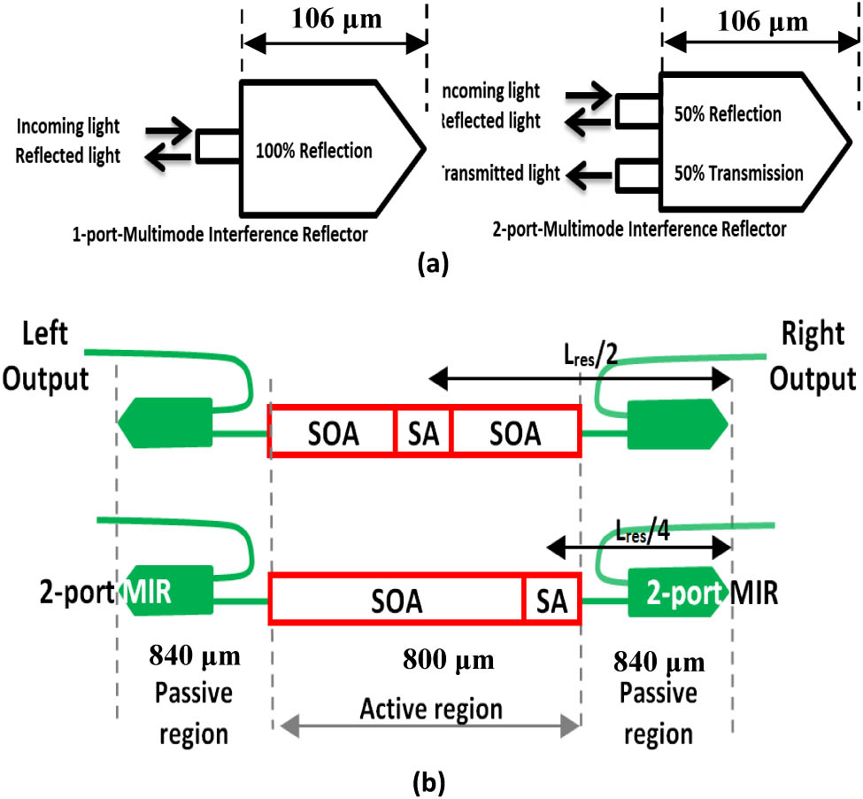
Figure 1.(a) Two types of MIRs; (b) two types of OCMLLD structures.

Figure 2.Photograph of two on-chip mode-locked lasers, using MIRs, with the SA at the two different locations.
The characterization setup is shown in Fig. 3, in which the thermoelectric control (TEC) sets the operation temperature at 17 °C. The chips are mounted on copper carriers, with submount boards to give electrical access to the pads through bond wires. The light output from the angled facets is collected through lensed fibers with an AR coated tip, spliced to an optical isolator followed by a 90/10 splitter. The 10% output is taken to a power meter, and the 90% output either to a Yokogawa AQ6370B optical spectrum analyzer, a high speed photodiode connected to an electrical spectrum analyzer, or an optical autocorrelator. The results correspond to a sample designed for a total resonator length , having as fundamental frequency 18 GHz. The active region lengths in the MPW run are fixed to 800 μm, using 780 μm for the SOA and 20 μm for the SA. The SA, as shown in Fig. 2, is on the right end of the active waveguide. This location was intended to be 600 μm away from the right-hand side MIR, to place the SA at and set the device operation at its fourth harmonic (72 GHz) [15]. Further details of the fabrication process belong to the SMART_Photonics InP generic foundry [16].
Figure 3.Experimental setup: AC, autocorrelator; EDFA, erbium doped fiber amplifier; ESA, electrical spectrum analyzer; I, current source; Iso, optical isolator; OSA, optical spectrum analyzer; PC, polarization controller; PD, photodiode; PM, power meter; −V, reverse bias voltage.
The optical power versus input current characteristic ( curve) is shown in Fig. 4(a), traced when the input current is swept for a fixed SA reverse voltage (). The threshold current is found to be 38 mA. As the current is swept to measure the optical power, the optical spectrum is measured simultaneously, shown in Fig. 4(b). From Figs. 4(a) and 4(b), we observe that the device presents different modes of operation. Close to threshold, the device operates as a Fabry–Perot laser, exhibiting lasing on several modes. Above a current level (50 mA), the device enters into a mode-locked state. A detailed view of the optical spectrum in the mode-locked state is shown in Fig. 5, when the bias conditions are and . The center wavelength is located around 1558 nm, and the inset of Fig. 5 shows a mode spacing of 16.7 GHz (0.134 nm). This evidences that the device is not working at the intended harmonic frequency, but at its fundamental (16.7 GHz), different from the designed target, revealing the uncertainty at the design phase of establishing the optical length of the MIR. This uncertainty has an impact on the location of the SA for colliding pulse mode-locking, and we have reached mode-locking at the fundamental frequency. However, using this frequency, we are able to establish that the optical length of the resonator is 2480 μm, from which the optical length of the MIR can be calculated to be 106 μm for future designs.
Figure 4.(a) Optical power versus current ( curve); regions are FP, Fabry–Perot; ML, mode-locked; (b) optical spectra map.
Figure 5.Optical spectrum of the OCMLLD in the mode-lock state; central wavelength, 1558 nm; span, 30 nm; inset shows the frequency mode spacing; resolution is 0.02 nm.
Following this analysis, the optical signal output was injected into an XPDV2020R U2 T high-speed photodiode with 40 GHz bandwidth to convert into a RF signal, measuring the electrical spectrum using an Anritsu MS2668C electrical spectrum analyzer. We observe the position and power of the repetition frequency, shown in Fig. 6, for the same conditions in which the optical spectrum was shown, and . In accordance with the frequency spacing of the optical modes, the fundamental frequency appears at , 47 dB over the noise floor. The linewidth of the beating RF spectrum fitted to a Lorentzian line-shape at full-width half-maximum (FWHM) is 91.90 kHz.
Figure 6.Electrical spectrum of the OCMLLD; center frequency, 15 GHz; span, 30 GHz; resolution bandwidth (RBW), 1 MHz; video bandwidth (VBW), 1 MHz.
The existence of optical pulses is analyzed using an intensity autocorrelation measurement, with an Applied Physics and Electronics (APE) Pulse-Check background-free autocorrelator. The pulse widths have been measured for varying current injection levels into the SOA () and reverse voltages on the SA (), showing the measured data in Figs. 7(a) and 7(b), respectively. We observe the same trends as in other mode-locked structures in which pulses broaden with increasing injection current, usually attributed to self-phase modulation (SPM), and shorten with increasing absorber reverse voltage, when the absorber recovery time is shortest [17]. The shortest pulse-width that has been measured is 1.72 ps with reverse bias to the absorber and 50 mA to the gain section (current level needed for the onset of mode-locking). In order to provide a detail of the pulse shape, Fig. 7(c) presents the autocorrelator output for the bias conditions in which we have shown the optical and electrical spectra, and . The measured trace has its best fit using a Gaussian pulse shape, from which we obtain that the pulse width is 2.92 ps. Furthermore, this allows us to calculate the time–bandwidth product (TBP), obtaining 0.49, close to that of a Fourier-transform limited Gaussian pulse (0.4413).
Figure 7.(a) Pulsewidth versus gain section current level at fixed ; (b) pulse width versus reverse absorber voltage at fixed ; (c) measured optical pulse shape (blue, line marked with circles) fitted to a Gaussian lineshape (red, continuous line).
In conclusion, we report for the first time to the best of our knowledge a novel fully monolithic mode-locked laser diode using MIRs. The device has been shown to operate at the fundamental repetition rate, from the optical and RF spectra. This is attributed to the uncertainty in the optical length of the novel MIRs, critical to achieve harmonic regimes by colliding pulse mode-locking. Measurements of the pulse shape show pulse widths from 1.72 to 4.39 ps. The greatest advantage of this device is that it does not required cleaved facets, and can be freely located on a PIC. This device has been fabricated in a MPW run, using active/passive technology which allows integration of this component with various other BBs to include additional functionalities.
References
[1] M. Smit, X. Leijtens, E. Bente, J. Van der Tol, H. Ambrosius, D. Robbins, M. Wale, N. Grote, M. Schell. Generic foundry model for InP-based photonics. IET Optoelectron., 5, 187-194(2011).
[2] K. A. Williams, M. G. Thompson, I. H. White. Long-wavelength monolithic mode-locked diode lasers. New J. Phys., 6, 179(2004).
[3] X. Guo, A. H. Quarterman, V. F. Olle, A. Wonfor, R. V. Penty, I. H. White. Variable repetition rate monolithically integrated mode-locked-laser-modulator-MOPA device. 23rd International Semiconductor Laser Conference (ISLC)(2012).
[4] L. Hou, M. Haji, B. Qiu, A. C. Bryce. Mode-locked laser array monolithically integrated with MMI combiner, SOA, and EA modulator. IEEE Photon. Technol. Lett., 23, 1064-1066(2011).
[5] J. Akbar, L. Hou, M. Haji, R. Dylewicz, M. J. Strain, J. H. Marsh, A. C. Bryce, A. E. Kelly. High average power (200 mW) 40 GHz mode-locked DBR lasers with integrated tapered optical amplifiers. Conference on Lasers and Electro-Optics (CLEO), CW1N.7(2012).
[6] S. Joshi, N. Chimot, R. Rosales, S. Barbet, A. Accard, A. Ramdane, F. Lelarge. Mode locked InAs/InP quantum dash based DBR Laser monolithically integrated with a semiconductor optical amplifier. International Conference on Indium Phosphide and Related Materials (IPRM)(2013).
[7] J. P. Hohimer, G. A. Vawter. Passive mode locking of monolithic semiconductor ring lasers at 86 GHz. Appl. Phys. Lett., 63, 1598-1600(1993).
[8] H. Cao, H. Deng, H. Ling, C. Liu, V. A. Smagley, R. B. Caldwell, G. Smolyakov, A. L. Gray, L. F. Lester, P. G. Eliseev, M. Osinski. Unidirectional operation of quantum-dot ring lasers. Conference on Lasers and Electro-Optics (CLEO), 3, 1793-1795(2005).
[9] M. Tahvili, Y. Barbarin, X. Leijtens, T. de Vries, E. Smalbrugge, J. Bolk, H. Ambrosius, M. Smit, E. Bente. Directional control of optical power in integrated InP/InGaAsP extended cavity mode-locked ring lasers. Opt. Lett., 36, 2462-2464(2011).
[10] L. Hou, M. Haji, J. H. Marsh. Monolithic mode-locked laser with an integrated optical amplifier for low-noise and high-power operation. IEEE J. Sel. Top. Quantum Electron., 19, 1100808(2013).
[11] E. Kleijn, M. K. Smit, X. J. M. Leijtens. Multimode interference reflectors: a new class of components for photonic integrated circuits. J. Lightwave Technol., 31, 3055-3063(2013).
[12] J. Zhao, E. Kleijn, P. J. Williams, M. K. Smit, X. J. M. Leijtens. On-chip laser with multimode interference reflectors realized in a generic integration platform. Compound Semiconductor Week (CSW/IPRM), 2011 and 23rd International Conference on Indium Phosphide and Related Materials, 1-4(2011).
[13] L. Xu, X. J. M. Leijtens, B. Docter, T. De Vries, E. Smalbrugge, F. Karouta, M. K. Smit. MMI-reflector: a novel on-chip reflector for photonic integrated circuits. 35th European Conference on Optical Communication (ECOC), 1-2(2009).
[14] D. J. Jones, L. M. Zhang, J. E. Carroll, D. D. Marcenac. Dynamics of monolithic passively mode-locked semiconductor lasers. IEEE J. Quantum Electron., 31, 1051-1058(1995).
[15] T. Shimizu, I. Ogura, H. Yokoyama. 860 GHz rate asymmetric colliding pulse mode locked diode lasers. Electron. Lett., 33, 1868-1869(1997).
[16]
[17] K. Merghem, A. Akrout, A. Martinez, G. Moreau, J.-P. Tourrenc, F. Lelarge, F. Van Dijk, G.-H. Duan, G. Aubin, A. Ramdane. Short pulse generation using a passively mode locked single InGaAsP/InP quantum well laser. Opt. Express, 16, 10675-10683(2008).


